ALLPCB


 1. Introduction
RF PCB design is often described as a "black art" because many theoretical aspects remain uncertain in public literature. For circuits operating below microwave frequencies (including low-frequency and low-speed digital circuits), careful planning and a solid understanding of design principles usually enable first-time success. For circuits at or above microwave frequencies and high-speed PC-class digital circuits, 2–3 PCB iterations are often required to achieve satisfactory performance. RF circuits above microwave frequencies typically require even more iterations and experienced designers, which illustrates the challenges of RF circuit design.
2. Common issues in RF circuit design
2.1 Interference between digital and analog modules
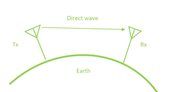
If analog (RF) and digital modules operate separately, each may function correctly. However, when placed on the same PCB and powered from the same supply, the overall system can become unstable. Digital signals switch frequently between ground and the positive supply (>3 V) with very short periods, often on the order of nanoseconds. The large amplitude and fast edges introduce abundant high-frequency components that are not limited to the basic switching frequency. In the analog RF path, signals from tuning circuits to the receiver are often below 1 μV, so the difference between digital and RF signal levels can reach about 120 dB. If digital and RF signals are not well separated, the tiny RF signals can be corrupted, degrading or disabling wireless functionality.
2.2 Power supply noise
RF circuits are sensitive to supply noise, especially voltage spikes and other high-frequency harmonics. Modern microcontrollers implemented in CMOS draw short bursts of current every internal clock cycle. For example, if a microcontroller runs at 1 MHz it will draw current at that frequency. Without proper power-supply decoupling, this can create voltage spikes on the supply rails. If those spikes reach RF circuit supply pins, they can cause serious malfunction.
2.3 Improper grounding
Poor ground handling in RF circuits can produce unexpected behavior. In many digital designs, circuits may function acceptably even without a ground plane. At RF frequencies, however, even a short ground trace behaves like an inductor. Roughly, inductance is about 1 nH per millimeter; at 433 MHz, a 10 mm PCB trace has a reactance of about 27 Ω. Without a ground plane, ground traces tend to be long and the circuit will not exhibit the intended performance.
2.4 Antenna radiation coupling to other analog circuits
A PCB often contains other analog subsystems such as ADCs or DACs. The high-frequency energy radiated by a transmitter antenna can reach ADC analog inputs because any trace can radiate or receive RF. If ADC inputs are not handled properly, RF may excite ESD diodes or other input circuitry, causing ADC errors or offset.
3. RF layout principles and solutions
3.1 RF layout concepts
When designing RF layouts, prioritize the following principles:
- Isolate high-power RF amplifiers (HPAs) from low-noise amplifiers (LNAs); keep high-power transmit circuits physically distant from low-power receive circuits.
- Provide large contiguous ground copper under high-power regions, preferably without vias; larger copper areas are better.
- Implement proper circuit and power-supply decoupling.
- Keep RF outputs physically separated from RF inputs.
- Keep sensitive analog signals as far as possible from high-speed digital and RF signals.
3.2 Physical partitioning and electrical partitioning
Partitioning can be divided into physical and electrical aspects. Physical partitioning addresses component placement, orientation, and shielding. Electrical partitioning covers power distribution, RF routing, sensitive circuits and signals, and grounding.
3.2.1 Physical partitioning principles
Component placement. Component placement is key to good RF design. Fix components on critical RF paths first and orient them to minimize RF path length, keeping inputs away from outputs and separating high-power and low-power circuitry where possible.
PCB stackup. A common effective stackup places the main ground plane on layer 2 beneath the top layer, and routes RF traces on the top layer. Minimize via size and count on RF paths to reduce inductance, reduce unwanted via stubs in the ground plane, and lower the chance of RF energy leaking into interior layers.
RF devices and routing. In physical layout, linear multi-stage amplifiers can help isolate RF regions, but duplexers, mixers, and IF amplifiers/mixers often carry multiple RF/IF signals and can interfere with each other. Route RF and IF traces to cross rather than run in parallel when possible, and separate them with ground between traces. Correct RF path routing is critical to overall PCB performance and typically consumes much of the layout time in cell phone PCB design.
Reducing coupling between high- and low-power devices. For example, place LNA circuits on one side of the board and HPAs on the other, connecting them via duplexers to shared RF front-ends and antennas. Use techniques to prevent vias from transferring RF energy between board faces; blind vias on both sides are commonly used. Arrange vias in areas not affected by RF to minimize adverse effects.
3.2.2 Electrical partitioning principles
Power transmission. In many handheld designs DC currents are small, so trace width is often not a limiting factor. However, HPA supplies require a dedicated wide high-current trace to minimize voltage drop. Use multiple vias to transfer current between layers to reduce loss.
Decoupling for high-power devices. If an HPA is not adequately decoupled at its supply pins, high-power noise can radiate across the board and cause multiple issues. Grounding for high-power devices is critical and often requires a metal shield can.
RF input/output isolation. It is essential to keep RF outputs away from RF inputs for amplifiers, buffers, and filters. If output feeds back to input at certain phase and amplitude, the stage can oscillate. At best, inadequate isolation causes instability, added noise, and intermodulation.
Filter I/O isolation. If RF traces loop from a filter input back to its output, the filter passband can be severely degraded. To achieve good isolation, surround the filter with ground, provide a grounded region under the filter connected to the main ground, and keep signals that must pass through the filter pins as far from the filter body as practical. Be careful with grounding across the board, as inadvertent ground connections can introduce unwanted coupling paths.
Digital and analog isolation. Keep digital circuits physically separated from analog circuits wherever possible. A proper analog ground and grounds used for shielding and signal separation are equally important. Small design changes from negligence can force a redesign. Keep RF traces away from analog traces and critical digital signals. Surround RF traces, pads, and components with grounded copper and connect it to the main ground. If an RF trace must cross other signal traces, run a grounded layer alongside the RF trace or ensure crossings occur at right angles to minimize capacitive coupling. Fill ground around RF traces and connect to the main ground. Minimize parallel run length between RF traces to reduce inductive coupling.
4. Conclusion
Rapid advances in RF integrated circuits offer broad opportunities for engineers working on wireless communication. At the same time, RF circuit design requires practical experience and engineering judgment. The summarized practices in this article can help RF IC developers shorten development cycles, avoid unnecessary detours, and save resources.