ALLPCB


Overview
The industry sees advanced packaging options emerging rapidly to pursue integration beyond Moore and higher levels of functional density. These packages concentrate many high-density interconnects and introduce both new and familiar design and reliability challenges.
First-generation fine-pitch multi-die packages used silicon interposers with through-silicon vias (TSVs) to deliver significant performance improvements, although they have limitations at higher RF frequencies (4 to 6 GHz) and the silicon interposer adds substantial cost. This spurred alternative approaches such as silicon bridges and high-density fan-out on substrate, each with trade-offs.
To produce high-yield modules that include many small dies, chip makers are extending existing processes and leveraging fan-out and embedded configurations. They are also addressing advanced packaging design challenges that require assembly process design kits (PDKs) analogous to those used for IC design.
Packaging and EDA Collaboration
The diversity of architectures in advanced packaging and the high cost of failures are driving closer collaboration between device design flows and outsource semiconductor assembly and test (OSAT) facilities. EDA vendors and OSATs are developing collaborative toolsets to improve package performance, reduce cost, and shorten time to integrate complex packages.
Co-development appears necessary for multi-die packages, especially when integrating dies from different suppliers. “There are no born 3D engineers. 2D engineers must quickly become 2.5D and 3D engineers,” said Shekhar Kapo, senior director of product management at Synopsys.
“In the SoC domain, methods, reference flows, and PDKs have evolved over many years and we rely on them for design. When you assemble all of these parts, you cannot treat the package engineer’s work as separate from the chip engineer’s work; you have to consider them together,” Kapo added.
John Park, director of product management for Custom IC and PCB at Cadence, noted that chip designers typically design against a foundry PDK, which provides libraries, sign-off design rules, and connectivity verification. For advanced packaging, similar automation and shared data are needed so engineers can focus on new designs and features rather than spending excessive time on one-off packaging composed of many discrete components.
“Design tools are increasingly able to treat the package as a single integrated design,” said Mike Kelly, vice president of Die/FCBGA integration at Amkor Technology. “With advanced packaging you still need timing sign-off when you have multiple dies. 3D adds another element because the package is inherently three-dimensional in the physical world. The challenge is to abstract it into forms compatible with Verilog and IC design tools. It is not yet 100% solved, but major customers are making it work.”
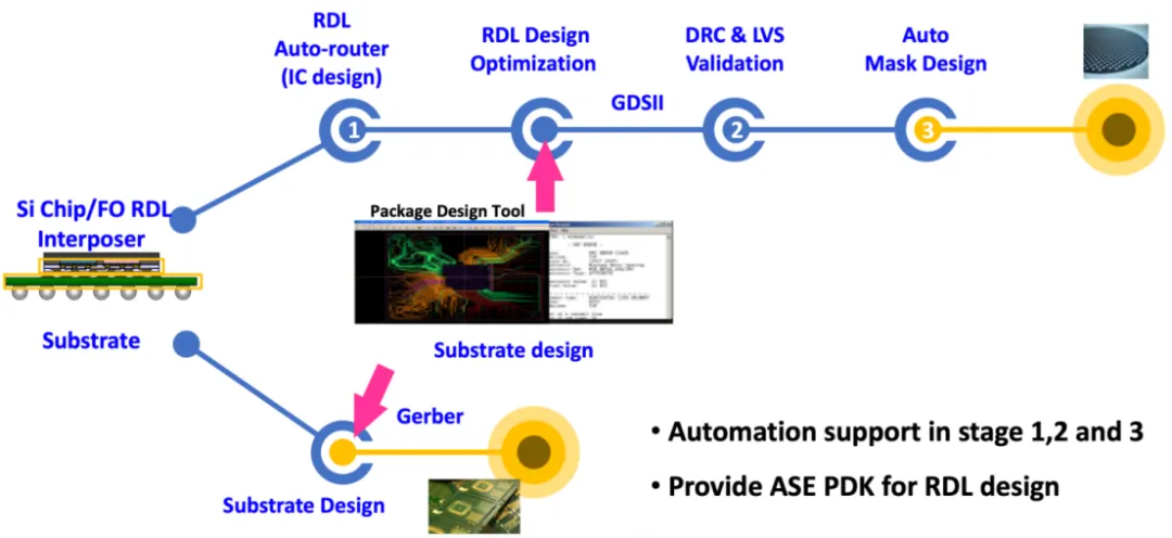
Greater automation also improves quality and reduces co-development time. For substrate design, an APD file can be used to generate Gerber output and then routing can proceed. ASE’s RDL design flow uses three automated routing steps to optimize RDL designs, then generates GDS. From the GDS, LVS (layout versus schematic) and DRC (design rule check) are run, and an automated mask design tool produces the masks. This automated routing approach can reduce layout cycle time by about 50%.
Using an automated mask generator alone can cut processing time from around three days to about one hour, according to ASE.
Interconnect Challenges
The number of electrical interconnects in packages is growing rapidly, raising reliability concerns. “Even a typical 2.5D design can easily contain 400k to 500k bumps. Because these are micro-bumps, they cannot tolerate high shear stress,” said Marc Swinnen, product marketing at Ansys. “When hot spots form, solder softens and without sufficient support the assembly will begin to warp and shift. Reliability is a major concern. Companies must run mechanical simulations of warpage and bending under thermal and mechanical stress, which directly affect field reliability and expected lifetime.”
Device makers are optimizing chip-to-chip and chip-to-package interconnects across architectures—whether built vertically with micro-bumps, hybrid bonding, and bridges, or horizontally with fan-out redistribution layers (RDL). Decisions about how and where to form interconnects are becoming central to package integration.
“Advanced packaging needs very high-density interconnect structures to combine multiple dies and make the system behave as if it were integrated on a single die,” said Eric Beyne, senior researcher and VP R&D at imec and program director for 3D system integration. “Efforts are focused on standardizing die-to-die communication with HBM, wire-based schemes, or UCIe. These standards need to guide how silicon interposers, silicon bridges, and high-density RDL combine, since very high-density interconnects are required for low-power operation.”
For high-performance applications, high bandwidth between dies is critical. “Higher-bandwidth die-to-die interconnects tend to be wide, low-power interfaces, so you need a relatively high-density interposer or interconnect layer to achieve them. That is a key differentiator for the packaging industry,” Kelly said.
Thermal modeling in advanced packages helps identify potential failure points; thermal issues and interconnect failures are among the leading causes of system faults. “Heat often leads to interconnect failure,” Swinnen noted.
New failure modes have appeared. “Low-k dielectric cracking is increasingly seen,” said Kelly Morgan, senior chief applications engineer for Sherlock at Ansys. “Solder solidifies around 230 C and CTE mismatch between low-k dielectrics and solder can generate torque on interconnects, imposing tensile stress on ultra-low-k layers and leading to cracks.”
Simulations of chemical and mechanical changes at early design stages can prevent such failures.
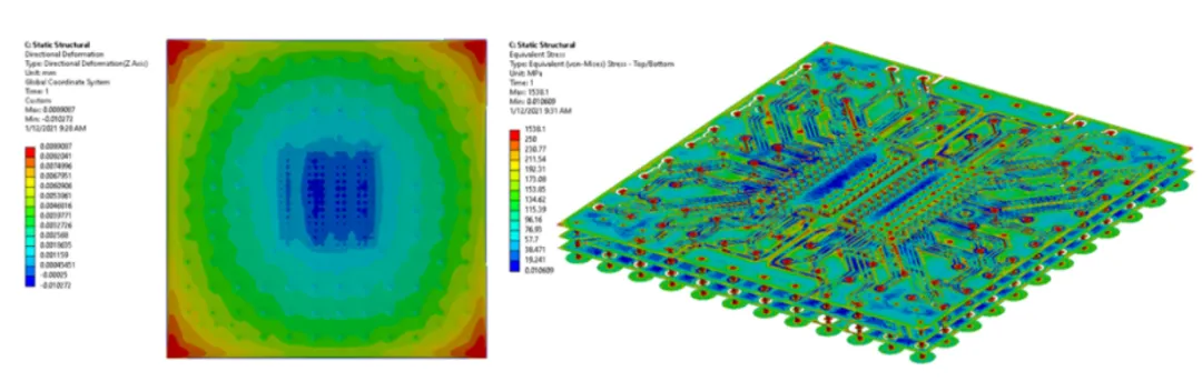
Thermal and mechanical characteristics should be considered early in the design phase to understand package behavior under temperature, vibration, or harsh environment cycles. For example, two adjacent dies may have different thermal movement but, due to proximity, can exhibit similar behavior.
“When assessing package reliability we always consider thermal cycling,” Kelly said. “CTE mismatches generate stress during cooling and heating. Chips are placed close to each other to avoid making interposers larger than necessary, because size is a cost factor. As a result, mold compounds may not see identical thermal histories.”
CTE mismatch between materials in different stacks has always been problematic, and for multiple packages on a substrate—especially in asymmetric layouts—the effects can be more severe. Optimal CTE match is silicon-to-silicon (wafer hybrid bonding) or silicon-to-silicon interposer (SiO2/copper). Silicon (≈2.5 ppm/K) and organic interposers (BT, CTE ≈15–16 ppm/K) are poorly matched.
Because roughly 90% of heat originates in the semiconductor, thermal interface materials (TIM) are typically placed between the package and the heatsink to provide a thermal path. TIMs also absorb some strain from CTE mismatches among die, substrate, and heatsink during assembly and field use.
TIM materials include adhesives, gels, and greases—most are polymer-based (epoxy or silicone) filled with conductive particles such as aluminum, alumina, zinc oxide, or silver. These materials offer high elongation and manufacturability, but their thermal conductivity is generally limited to about 10 W/m-K. Engineers are evaluating higher-conductivity solutions such as gallium-indium alloys, gallium-indium-tin, graphene, and even metal TIMs for high-power applications.
Soldering presents both challenges and solutions at advanced nodes. Below approximately 10 um pitch, the industry is expected to use hybrid bonding for copper-copper pad connections. Hybrid bonding methods such as thermal compression bonding (TCB) help achieve high-quality bonds despite some warpage, and using non-conductive paste/film (NCP/NCF) with TCB addresses challenges like cavity filling or pre-dispensed underfill for large dies with small pitches.
A potential drawback is that as pitches shrink, the forced behavior of solder during TCB between copper pillars and die pads can cause solder extrusion and shorting.
As interconnect methods evolve, companies are collaborating to resolve manufacturing issues. For example, UMC is working with Cadence, Winbond, Faraday, and ASE to develop a wafer-to-wafer (W2W) 3D-IC platform. By combining expertise across vendors in design, manufacturing, 3D-ICs, testing, and packaging, the group aims to address 3D challenges such as vertical integration design flows, W2W hybrid bonding alignment, and validated test and assembly paths for 3D stacking, targeting end-to-end solutions with system-level validation.
Fan-Out Wafer-Level Packaging (FOWLP)
Fan-out packaging offers smaller, thinner footprints and improved electrical and thermal performance compared with existing flip-chip approaches. High-density fan-out RDL comes in two primary types: die-first and die-last. The processes differ slightly and each has advantages and disadvantages.
In die-first, a temporary carrier with a thermal release tape is prepared, known-good-dice (KGD) are placed on the carrier, molding is performed, then the carrier is released, RDL is formed, solder bumps are added, and the parts are singulated. In die-last, a release layer is first deposited, then RDL is built; known-good molded units are aligned, followed by molding, carrier release, ball deposition, and singulation.
Although die-last offers significant yield advantages, die-first is the more mature approach.
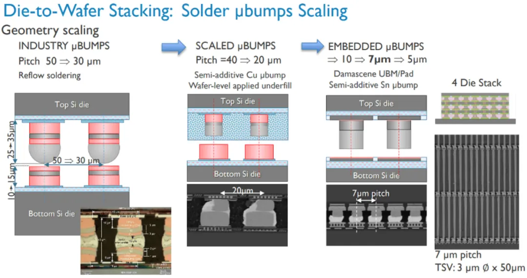
“Die-first can provide slightly better performance because the die signal connects directly into the RDL. But yield concerns may drive choices toward die-last FOWLP,” said ASE. Current micro-bump pitches range from about 55 to 40 um, with 35 um under development; die-first eliminates the need for micro-bumps and can reduce die-to-die spacing to about 25 um.
Yield limits associated with scaling micro-bumps have encouraged development of hybrid bonding methods that directly connect copper pads. However, the high cost and complexity of hybrid bonding are also motivating efforts to manufacture smaller bumps. imec expects that half-additive copper micro-bump schemes with wafer-level underfill could scale current pitch limits of about 35 um down toward 20 um. For sub-10 um scales, tin bumps and Cu/Sn pad stacks are used for pad-to-bump connections.
Conclusion
The push for higher-density interconnects in small-die integrated packages is driving more scalable approaches, including micro-bump scaling and hybrid bonding. Each package is effectively custom, which increases the engineering workload on the design side. As familiarity with options such as silicon and organic interposers, RDL fan-out, and embedded solutions grows, reliability—especially related to thermal and mechanical analysis—becomes a priority.
Integration challenges now span design, manufacturing, test, and assembly, and collaborative efforts among EDA vendors, foundries, memory and system suppliers, and OSATs are becoming more common. Industry progress toward integrating small dies from multiple suppliers into packages appears inevitable as these collaborative ecosystems mature.