ALLPCB


In the fast-evolving world of electronics, High-Density Interconnect (HDI) PCBs are at the heart of modern devices like smartphones, wearables, and medical equipment. When it comes to creating the tiny holes, or vias, needed for these compact boards, laser drilling stands out as the superior choice over traditional mechanical drilling. Why? Laser drilling offers unmatched precision, supports microvia technology, and meets the demands of miniaturization in HDI PCB manufacturing. In this blog, we’ll dive deep into the differences between laser drilling vs mechanical drilling for PCBs, explore why laser drilling is critical for HDI designs, and break down the key benefits and methods of PCB drilling.
What Are HDI PCBs and Why Do They Matter?
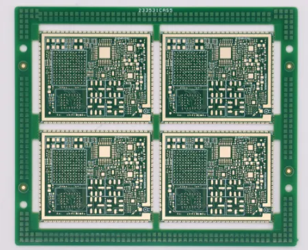
HDI PCBs are specialized circuit boards designed to pack more components into a smaller space. They achieve this through finer lines, tighter spacing, and smaller vias—often called microvias—that connect multiple layers. These boards are essential for high-performance electronics where size and speed are critical. For instance, a typical HDI PCB might feature microvias with diameters as small as 0.1 mm (100 microns), allowing for signal speeds up to 10 Gbps in advanced applications.
The challenge with HDI PCB manufacturing lies in creating these tiny, precise holes without damaging the board or compromising its integrity. Traditional mechanical drilling struggles to meet these requirements, which is where laser drilling becomes indispensable.
Laser Drilling vs Mechanical Drilling for PCBs: A Side-by-Side Comparison
Understanding the differences between laser drilling and mechanical drilling is key to appreciating why laser technology is the go-to choice for HDI PCBs. Let’s break it down:
1. Precision and Size of Holes
Mechanical drilling uses a rotating drill bit to create holes in a PCB. While effective for larger through-holes (typically 0.3 mm and above), it struggles with the ultra-small microvias required for HDI designs. Drill bits can wander or break at such small scales, leading to inconsistent hole sizes or damage to the board.
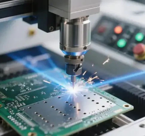
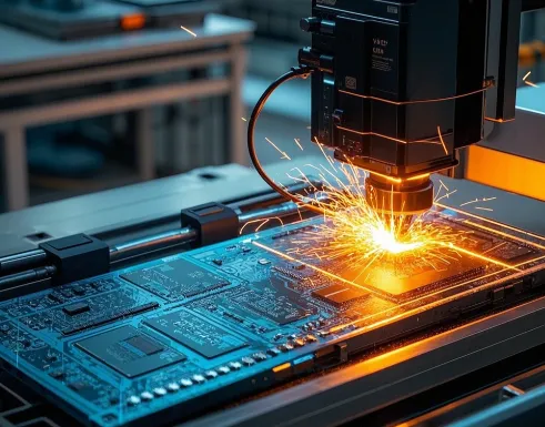
Laser drilling, on the other hand, uses a focused beam of light to vaporize material with pinpoint accuracy. It can create holes as small as 0.05 mm (50 microns) in diameter, perfect for microvia technology. This precision ensures that the tight spacing and fine pitch of HDI components are maintained without errors.
2. Material Compatibility
Mechanical drilling generates heat and friction, which can cause delamination or cracking in delicate materials like thin laminates or flexible substrates often used in HDI PCBs. Laser drilling is a non-contact process, meaning there’s no physical stress on the board. It can handle a wide range of materials, from standard FR-4 to advanced high-frequency laminates, without risking damage.
3. Speed and Efficiency
For high-volume production, laser drilling often outpaces mechanical methods when creating microvias. A single laser system can drill thousands of holes per second—some advanced systems achieve up to 9,000 vias per second—while maintaining consistent quality. Mechanical drilling, while faster for larger holes, requires frequent tool changes and setup adjustments for smaller vias, slowing down the process.
4. Cost Considerations
At first glance, laser drilling equipment may seem more expensive due to the initial investment in high-tech systems. However, the reduced need for tool replacement, lower risk of board damage, and higher throughput often make it more cost-effective for HDI PCB manufacturing in the long run. Mechanical drilling might be cheaper for simpler boards with larger holes, but it falls short when precision and density are priorities.
Why Laser Drilling is Essential for HDI PCB Manufacturing
HDI PCBs are defined by their need for high component density and complex interlayer connections. Here’s why laser drilling is not just an option but a necessity for these advanced boards:
1. Enabling Microvia Technology
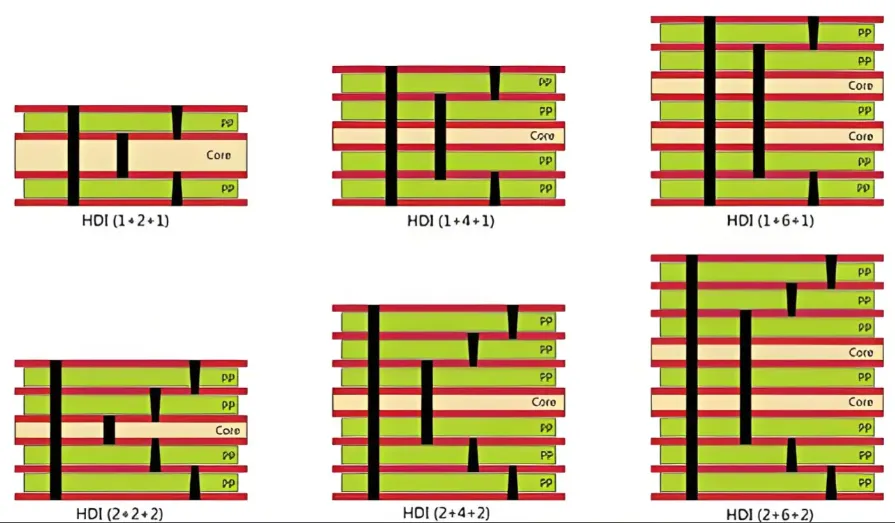
Microvias are the backbone of HDI designs, allowing connections between closely stacked layers without taking up much space. These vias are often blind (connecting an outer layer to an inner one) or buried (connecting inner layers only), with depths typically less than 0.25 mm. Laser drilling is the only reliable method to achieve such controlled depth and small diameters. For example, a microvia with a 0.1 mm diameter and a 1:1 aspect ratio (depth equal to diameter) is standard in HDI boards, and only laser systems can consistently produce this.
2. Supporting Miniaturization Trends
As devices get smaller, so do the PCBs inside them. HDI boards often support fine-pitch components like Ball Grid Arrays (BGAs) with pitches as tight as 0.3 mm. Laser-drilled microvias allow for via-in-pad designs, where the via is placed directly under the component pad to save space. This is impossible with mechanical drilling due to size limitations and alignment issues.
3. Improving Signal Integrity
In high-speed applications, signal integrity is critical. HDI PCBs often handle frequencies above 1 GHz, where even small imperfections in vias can cause signal loss or interference. Laser drilling creates smooth, uniform holes with minimal residue, reducing impedance mismatches. For instance, a poorly drilled via might introduce a parasitic capacitance of 0.5 pF, disrupting a 5 Gbps signal, while a laser-drilled via maintains tighter tolerances for consistent performance.
Understanding PCB Drilling Methods: Laser Technology in Depth
Laser drilling isn’t a one-size-fits-all solution. Different types of lasers and techniques are used depending on the PCB material and design requirements. Here’s a closer look at how it works:
Types of Lasers Used in PCB Drilling
- CO2 Lasers: These are commonly used for drilling through dielectric materials like epoxy resin in PCBs. They operate at a wavelength of 10.6 microns and are ideal for removing organic material with minimal heat damage to surrounding areas.
- UV Lasers: With a shorter wavelength (around 355 nm), UV lasers excel at drilling through copper and other metals. They provide high precision for microvias and are often used in combination with CO2 lasers for multilayer HDI boards.
- Fiber Lasers: These are newer to the PCB industry but are gaining traction for their ability to drill at high speeds with excellent beam quality. They’re often used in advanced manufacturing setups for both metal and dielectric layers.
Laser Drilling Techniques
- Percussion Drilling: The laser fires short, intense pulses to remove material layer by layer. This is ideal for creating deep microvias with controlled depth.
- Trepanning: The laser beam moves in a circular pattern to cut out larger holes. This method is less common for microvias but useful for specific via sizes in HDI designs.
- Helical Drilling: The beam spirals inward to create a hole, offering a balance between speed and precision for certain applications.
These techniques allow manufacturers to tailor the drilling process to the specific needs of an HDI PCB, ensuring optimal results for complex designs.
Key Benefits of Laser Drilling for HDI PCBs
Beyond precision and compatibility with microvia technology, laser drilling brings several advantages to HDI PCB manufacturing:
1. Reduced Risk of Defects: Since there’s no physical contact, there’s no wear on tools or risk of drill bit breakage. This leads to fewer defective boards and higher yields in production.
2. Flexibility in Design: Laser drilling supports complex via structures like stacked or staggered microvias, which are common in HDI boards with 6 or more layers. This flexibility allows engineers to push the boundaries of design.
3. Environmentally Friendly: Unlike mechanical drilling, which generates dust and debris, laser drilling produces minimal waste. The process is cleaner and aligns with sustainable manufacturing practices.
4. Scalability: As production volumes increase, laser systems can handle large batches with consistent quality, making them ideal for mass production of HDI PCBs used in consumer electronics.
Challenges and Limitations of Laser Drilling
While laser drilling is transformative for HDI PCB manufacturing, it’s not without challenges. Understanding these limitations helps in making informed decisions during the design and production phases.
1. Initial Cost: The upfront investment in laser drilling equipment is significant, which can be a barrier for smaller manufacturers. However, the long-term savings often outweigh this cost for high-volume HDI production.
2. Depth Limitations: Laser drilling is typically limited to shallow depths (less than 0.25 mm per pass), as deeper holes require multiple passes or alternative methods. This is why through-holes in thicker boards are still mechanically drilled.
3. Material Sensitivity: Certain materials may absorb laser energy differently, requiring careful calibration to avoid burning or incomplete drilling. Advanced systems mitigate this through adjustable parameters.
The Future of PCB Drilling Methods: Laser Takes the Lead
As electronics continue to shrink and performance demands grow, the role of laser drilling in PCB manufacturing will only expand. Emerging trends point to even faster, more precise laser systems capable of handling increasingly complex HDI designs. For instance, innovations in fiber laser technology are reducing drilling times while maintaining accuracy, making the process even more efficient.
While mechanical drilling will still have a place for simpler boards or larger holes, it’s clear that laser drilling is the future for high-density, high-performance applications. The ability to create microvias with diameters below 0.05 mm and support signal speeds beyond 10 Gbps positions laser technology as the cornerstone of modern PCB production.
Conclusion: Embracing Laser Drilling for HDI Success
In the race to build smaller, faster, and more reliable electronics, HDI PCBs are leading the charge—and laser drilling is the key to making them possible. By offering unparalleled precision, supporting microvia technology, and meeting the demands of miniaturization, laser drilling goes beyond the limitations of mechanical methods. For engineers and manufacturers, adopting this technology isn’t just a choice; it’s a necessity to stay competitive in a rapidly advancing industry.
At ALLPCB, we’re committed to leveraging cutting-edge solutions like laser drilling to deliver top-quality HDI PCBs for your projects. Whether you’re designing for consumer electronics, automotive systems, or medical devices, our expertise ensures your boards meet the highest standards of performance and reliability.