 ALLPCB


Hard gold plating is often associated with edge connectors in printed circuit boards (PCBs), but its applications in modern electronics extend far beyond this familiar use. From enhancing wearable devices to ensuring reliability in critical systems, hard gold plating plays a vital role in various innovative areas. In this blog, we’ll explore unexpected hard gold plating applications, dive into unique hard gold plating use cases, highlight hard gold plating innovative uses, discuss alternatives to hard gold plating, and examine its growing role in hard gold plating in wearable devices. Let’s uncover how this advanced finishing technique is shaping the future of electronics.
What Is Hard Gold Plating and Why Does It Matter?
Hard gold plating is a specialized electroplating process that deposits a thin layer of gold alloy, typically mixed with small amounts of cobalt or nickel, onto a surface. Unlike soft gold, which prioritizes purity for maximum conductivity, hard gold is engineered for durability and wear resistance. This makes it ideal for components that experience frequent contact, friction, or harsh environments.
In modern electronics, hard gold plating is prized for its excellent electrical conductivity, corrosion resistance, and ability to withstand repeated mechanical stress. With a typical hardness range of 130-200 Knoop, hard gold can endure up to 100,000 mating cycles in connectors, far surpassing other finishes. Its ability to maintain signal integrity, even at high frequencies (up to several GHz), is another reason it’s a go-to choice for engineers designing high-performance systems.
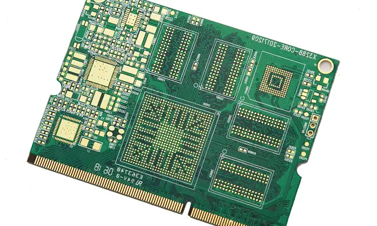
Traditional Use: Edge Connectors and Beyond
Before diving into unexpected applications, it’s worth noting the traditional role of hard gold plating in edge connectors. These are the gold-plated fingers on PCBs that plug into slots, such as those in computer motherboards or graphics cards. Hard gold ensures reliable electrical contact and protects against wear from repeated insertions, with typical thickness ranging from 30 to 50 microinches (0.76 to 1.27 micrometers) for optimal performance.
However, as electronics evolve, so do the demands on materials like hard gold. Let’s explore some surprising hard gold plating applications that go beyond the familiar edge connector.
Unexpected Applications of Hard Gold Plating in Modern Electronics
Hard gold plating is finding its way into diverse areas of electronics, driven by the need for reliability, miniaturization, and performance. Below are some standout hard gold plating use cases that showcase its versatility.
1. High-Reliability Aerospace and Defense Systems
In aerospace and defense electronics, failure is not an option. Hard gold plating is used in critical components like satellite connectors, avionics systems, and military-grade communication devices. These systems often operate in extreme conditions—temperatures ranging from -55°C to 125°C and high humidity—where corrosion or signal loss could be catastrophic. Hard gold’s resistance to oxidation and its ability to maintain low contact resistance (typically under 50 milliohms) make it indispensable.
For example, in satellite systems, hard gold-plated contacts ensure consistent signal transmission for data rates exceeding 10 Gbps, even after years of exposure to the vacuum of space. Its durability also reduces maintenance needs, a critical factor in environments where repairs are impossible.

2. Medical Electronics and Implantable Devices
Medical electronics, particularly implantable devices like pacemakers and neurostimulators, rely on hard gold plating for biocompatibility and long-term reliability. Hard gold is non-reactive with bodily fluids, preventing corrosion that could harm the patient or degrade the device. Its wear resistance is also crucial for connectors that must endure constant micro-movements within the body.
In these applications, hard gold layers as thin as 10 microinches (0.25 micrometers) are often used to balance cost with performance. This ensures that devices maintain stable impedance levels (often below 100 ohms) for accurate signal delivery, such as pacing signals in a pacemaker operating at 1-5 volts.
3. Automotive Electronics for Harsh Environments
Modern vehicles are packed with electronics, from engine control units to infotainment systems. Hard gold plating is increasingly used in automotive connectors and sensors exposed to vibration, temperature swings, and corrosive elements like road salt. Its ability to maintain signal integrity at high frequencies (up to 6 GHz in some radar systems) and resist fretting corrosion—caused by micro-movements—makes it ideal for these harsh conditions.
For instance, in electric vehicles, hard gold-plated contacts in battery management systems ensure reliable power distribution with minimal voltage drop, supporting currents as high as 100 amps in some configurations.
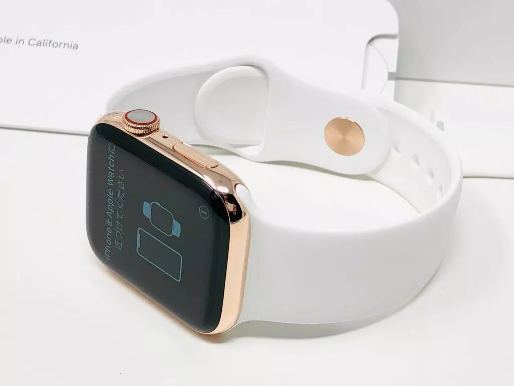
Hard Gold Plating in Wearable Devices: A Growing Trend
One of the most exciting areas for hard gold plating in wearable devices is in consumer electronics like smartwatches, fitness trackers, and hearables. Wearables face unique challenges: they must be lightweight, compact, and resistant to sweat, skin contact, and daily wear. Hard gold plating addresses these needs by providing durable, corrosion-resistant contacts in charging ports and sensor connections.
In a typical smartwatch, hard gold-plated pogo pins or spring contacts ensure consistent charging and data transfer, even after thousands of connections. With contact resistance as low as 30 milliohms, these components minimize power loss and heat buildup, extending battery life—a critical factor for devices with limited power capacity (often under 300 mAh).
Moreover, as wearables integrate more health-monitoring features like ECG or blood oxygen sensors, hard gold ensures precise signal transmission. For example, ECG sensors in wearables require low-noise contacts to detect millivolt-level signals accurately, and hard gold’s stable conductivity (with resistivity around 2.44 microohm-cm) is perfect for this task.
Innovative Uses of Hard Gold Plating in Emerging Technologies
As technology advances, hard gold plating innovative uses are emerging in cutting-edge fields. These applications highlight how hard gold adapts to the demands of next-generation electronics.
1. 5G and High-Speed Communication Systems
The rollout of 5G networks demands components that can handle ultra-high frequencies (up to 100 GHz) with minimal signal loss. Hard gold plating is used in RF connectors and microstrip lines within 5G base stations and devices. Its low dielectric loss and ability to maintain impedance stability (often within ±5% of target values like 50 ohms) ensure clear, high-speed data transmission.
Innovative designs also use hard gold in flexible PCBs for foldable smartphones, where durability during repeated bending (up to 200,000 cycles) is critical.
2. Internet of Things (IoT) Devices
IoT devices, from smart home sensors to industrial monitors, often operate in varied environments with limited maintenance. Hard gold plating on connectors and contact points ensures long-term reliability, with some devices rated for over 10 years of continuous operation. Its resistance to tarnishing also means IoT devices can maintain connectivity in humid or dusty conditions without signal degradation.
Alternatives to Hard Gold Plating: Exploring Other Options
While hard gold plating offers unmatched benefits, cost and specific application needs sometimes call for alternatives to hard gold plating. Below are a few options engineers consider, along with their trade-offs.
1. Electroless Nickel Immersion Gold (ENIG)
ENIG is a popular alternative, especially for PCBs where soldering is a primary concern. It consists of a nickel layer topped with a thin immersion gold layer (typically 2-5 microinches). While ENIG is cheaper and provides good solderability, it lacks the wear resistance of hard gold, making it unsuitable for high-mating-cycle applications (often failing after 1,000 cycles).
2. Palladium-Nickel with Gold Flash
This finish combines a palladium-nickel alloy with a thin gold flash layer. It offers similar corrosion resistance to hard gold and is often more cost-effective. However, its contact resistance (around 100 milliohms) is higher, which can impact high-frequency performance compared to hard gold’s lower values.
3. Silver Plating
Silver plating provides excellent conductivity (resistivity of 1.59 microohm-cm, better than gold’s 2.44 microohm-cm) and is less expensive. However, it tarnishes easily in humid or sulfur-rich environments, leading to signal degradation over time. This makes it less reliable for long-term applications compared to hard gold.
Challenges and Considerations with Hard Gold Plating
Despite its advantages, hard gold plating isn’t without challenges. Its higher cost—often 3-5 times more expensive than alternatives like ENIG—can be a barrier for budget-sensitive projects. Additionally, the plating process requires precise control to avoid issues like porosity, which can compromise corrosion resistance if not managed properly.
Engineers must also balance thickness with functionality. While thicker layers (above 50 microinches) enhance durability, they increase costs and may cause issues with solderability if the underlying nickel barrier layer is insufficient.
Future Outlook: Where Is Hard Gold Plating Headed?
The future of hard gold plating looks promising as electronics continue to push boundaries in performance and miniaturization. Emerging fields like quantum computing may leverage hard gold for ultra-low-noise contacts in cryogenic environments (below -200°C). Additionally, advancements in plating techniques, such as pulse plating, could reduce costs by optimizing gold usage without sacrificing quality.
In wearables and IoT, we expect to see even thinner hard gold layers—potentially under 10 microinches—paired with innovative alloys to maintain durability while cutting expenses. These developments will keep hard gold at the forefront of reliable, high-performance electronics.
Conclusion: The Versatility of Hard Gold Plating
Hard gold plating is far more than just a finish for edge connectors. Its unique blend of durability, conductivity, and corrosion resistance makes it a critical material in diverse areas, from aerospace systems to hard gold plating in wearable devices. Through hard gold plating innovative uses in 5G, IoT, and medical devices, it continues to meet the evolving demands of modern electronics. While alternatives to hard gold plating exist, few match its reliability in high-stakes applications.
At ALLPCB, we’re committed to helping engineers harness the power of advanced materials like hard gold to bring their designs to life. Whether you’re exploring hard gold plating applications for a new project or seeking cost-effective solutions, understanding these hard gold plating use cases can guide your decisions. Let’s build the future of electronics together with precision and innovation.


