 ALLPCB


If you're delving into multilayer PCB design, you've likely encountered the terms "blind vias" and "buried vias." These are specialized drilling techniques used to create connections between layers in a printed circuit board (PCB) without taking up unnecessary space on the surface. But what exactly are they, and how does mechanical drilling play a role in their creation? In this comprehensive guide, we'll explore advanced techniques in mechanical drilling for blind and buried vias, their importance in multilayer PCB design, and how they can optimize your projects for performance and space efficiency.
Whether you're an engineer working on high-density interconnect (HDI) boards or a designer looking to improve signal integrity, understanding these methods is crucial. Let's dive into the world of blind vias, buried vias, mechanical drilling, and their applications in multilayer PCBs.
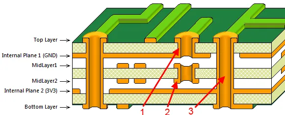
What Are Blind and Buried Vias in PCB Design?
Before we get into the advanced drilling techniques, let’s define the basics. Vias are small holes in a PCB that allow electrical connections between different layers. In traditional designs, through-hole vias go all the way from the top to the bottom of the board. However, in multilayer PCBs where space and performance are critical, blind and buried vias offer more efficient solutions.
- Blind Vias: These connect the outermost layer of a PCB to one or more inner layers but do not go through the entire board. For example, a blind via might link the top layer to the second layer, leaving the bottom layers untouched.
- Buried Vias: These are located entirely within the inner layers of a PCB and do not reach the outer surfaces. They might connect layer 2 to layer 3 in a six-layer board, for instance, without affecting the top or bottom surfaces.
Both types are essential for high-density designs, as they save surface space for components and reduce signal interference. Their creation, however, requires precision, which is where mechanical drilling comes into play.
Why Use Blind and Buried Vias in Multilayer PCB Design?
In modern electronics, devices are becoming smaller and more complex, demanding PCBs with higher component density and better performance. Blind and buried vias address these needs in several ways:
- Space Efficiency: By not extending through the entire board, these vias free up space on outer layers for additional components or routing.
- Improved Signal Integrity: Shorter via lengths reduce signal loss and crosstalk, which is critical for high-speed applications. For instance, in a design operating at 5 GHz, minimizing via stub length with blind vias can reduce signal reflection by up to 20%.
- Enhanced Design Flexibility: Designers can create more complex routing paths in multilayer PCBs, accommodating intricate circuits without increasing board size.
- Reduced Layer Count: Using these vias can sometimes eliminate the need for additional layers, lowering manufacturing costs. For example, a design that might require eight layers with through-hole vias could be reduced to six layers with strategic use of blind and buried vias.
These benefits make blind and buried vias indispensable for industries like telecommunications, aerospace, and consumer electronics, where performance and compactness are paramount.
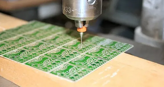
The Role of Mechanical Drilling in Creating Blind and Buried Vias
Mechanical drilling is a core process in PCB manufacturing, used to create holes for vias and component mounting. While laser drilling is often used for smaller microvias in HDI designs, mechanical drilling remains a reliable and cost-effective method for blind and buried vias, especially in boards with standard thicknesses (0.8mm to 3.2mm).
In the context of blind and buried vias, mechanical drilling requires advanced techniques to ensure precision and avoid damaging inner layers. Here's how it works:
- Sequential Lamination: For buried vias, the inner layers are laminated and drilled first before additional layers are added. This ensures the via is "buried" within the board.
- Controlled Depth Drilling: For blind vias, the drill must stop at a specific layer without penetrating further. This is achieved using depth-controlled drilling machines that can target a precision of ±0.05mm.
- Back Drilling: In some cases, through-hole vias are drilled first, then partially removed from the opposite side to create a blind via. This technique minimizes stub length, improving signal integrity for high-speed designs.
Mechanical drilling for these vias demands high-quality equipment and skilled operators to maintain accuracy. A slight misalignment or over-drilling can lead to connection failures or compromised board integrity.
Advanced Techniques in Mechanical Drilling for Blind and Buried Vias
As PCB designs grow more complex, manufacturers have developed advanced mechanical drilling techniques to meet the demands of multilayer boards. Below are some cutting-edge methods used to create blind and buried vias with precision and efficiency.
1. Depth-Controlled Drilling with Real-Time Monitoring
One of the biggest challenges in drilling blind vias is stopping at the correct depth. Modern drilling systems use real-time monitoring to detect when the drill reaches the target layer. Sensors measure parameters like torque and resistance, ensuring the drill stops within 0.02mm of the intended depth. This technique is critical for boards with tight tolerances, such as those used in 5G infrastructure, where signal paths must be exact to maintain impedance values around 50 ohms.
2. Multi-Step Drilling for Buried Vias
Creating buried vias often involves multiple drilling and lamination steps. After drilling the initial holes in the inner layers, copper plating is applied to form conductive paths. Additional layers are then laminated over these vias, hiding them within the board. Advanced drilling systems can handle multiple cycles with alignment accuracy of ±0.1mm, ensuring that buried vias connect the correct layers without shorts or opens.
3. High-Speed Drilling for Reduced Heat Build-Up
Drilling generates heat, which can damage the resin and copper in a PCB, especially in multilayer designs with thin dielectrics (as low as 0.1mm). High-speed drilling systems operate at spindle speeds up to 200,000 RPM, reducing contact time and heat build-up. This technique is particularly useful for boards with high layer counts (10+ layers), where thermal stress could warp the board or delaminate layers.
4. Automated Drill Path Optimization
Advanced drilling machines use software to optimize drill paths, minimizing tool wear and reducing production time. For complex multilayer PCBs with hundreds of vias, this can cut drilling time by up to 30%. Optimized paths also reduce the risk of drill bit breakage, which is a common issue when working on dense boards with small via sizes (down to 0.3mm in diameter).
Challenges in Mechanical Drilling for Blind and Buried Vias
While mechanical drilling offers many advantages, it comes with challenges that require careful attention during the design and manufacturing process.
- Alignment Issues: Misalignment between layers can result in vias that don’t connect properly. For a 10-layer board, even a 0.05mm shift can cause a connection failure.
- Drill Wear: Drilling through multiple layers of copper and dielectric material wears out drill bits quickly, especially for small-diameter vias. Worn bits can create rough holes, leading to poor plating and unreliable connections.
- Cost Considerations: The equipment and expertise required for advanced drilling techniques can increase manufacturing costs. For instance, depth-controlled drilling may add 10-15% to the overall production expense compared to standard through-hole drilling.
To overcome these challenges, designers must work closely with manufacturers during the early stages of PCB design to ensure that via placement and stackup are optimized for drilling capabilities.
Design Tips for Optimizing Blind and Buried Vias in Multilayer PCBs
Successful implementation of blind and buried vias starts with thoughtful design. Here are some practical tips to ensure your multilayer PCB design is compatible with advanced mechanical drilling techniques:
- Minimize Via Depth Variability: Keep blind vias to a consistent depth where possible. For example, if most blind vias connect layer 1 to layer 2, avoid designs where some connect to layer 3 unless necessary. This simplifies the drilling process.
- Use Standard Via Sizes: Stick to via diameters of 0.3mm or larger for mechanical drilling. Smaller sizes may require laser drilling, increasing costs.
- Plan Layer Stackup Carefully: Ensure that buried vias are placed in layers that can be laminated and drilled in sequence without affecting outer layers. A typical 6-layer stackup might place buried vias between layers 2 and 5 for balanced manufacturing.
- Account for Aspect Ratio: Maintain a via aspect ratio (depth to diameter) of 10:1 or lower to ensure reliable plating. For a 1.6mm thick board, this means via diameters should be at least 0.16mm.
By following these guidelines, you can reduce manufacturing errors and improve the reliability of your PCB.
Applications of Blind and Buried Vias in Modern Electronics
The use of blind and buried vias is widespread across industries that rely on compact, high-performance electronics. Here are a few examples:
- Smartphones and Tablets: These devices use HDI boards with blind vias to fit complex circuitry into thin form factors. A typical smartphone PCB might have over 1,000 vias, many of them blind or buried, to manage space constraints.
- Automotive Systems: Advanced driver-assistance systems (ADAS) require multilayer PCBs with high-speed signal paths. Buried vias help route signals between inner layers without interfering with surface-mounted sensors.
- Medical Devices: Wearable health monitors and diagnostic equipment often use blind vias to maintain a small footprint while ensuring reliable connections for critical data transmission.
Conclusion: Elevating PCB Design with Advanced Drilling Techniques
Blind and buried vias are game-changers in multilayer PCB design, offering space savings, improved signal integrity, and greater design flexibility. However, their creation relies heavily on advanced mechanical drilling techniques like depth-controlled drilling, multi-step processes, and high-speed systems. By understanding these methods and incorporating best practices into your design, you can take full advantage of these vias to create cutting-edge electronics.
At ALLPCB, we’re committed to supporting engineers and designers with the latest manufacturing technologies for multilayer PCBs. Whether you’re working on a high-density board for a consumer product or a complex system for industrial use, mastering blind and buried vias through precision drilling can elevate your projects to new heights. Let’s build the future of electronics together with innovative solutions tailored to your needs.


