ALLPCB


Overview
T/R stands for Transmit and Receive. A T/R assembly refers to the portion of a radio transmit/receive system between the transceiver and the antenna: one side of a T/R assembly connects to the antenna and the other side connects to the intermediate-frequency processing unit, forming a radio transceiver channel.
T/R modules are the basic components and a key technology for active phased-array radar antennas. They perform transmit-signal amplification, receive-signal amplification, and control of signal amplitude and phase. Typical internal elements include low-noise amplifiers (LNA), power amplifiers (PA), limiters, and phase shifters. An active phased array can contain thousands of T/R modules, which must deliver high power, high efficiency and low noise while minimizing size and weight.
These modules strongly influence array performance and require substantial packaging and integration work. T/R modules can account for roughly half of an active phased-array antenna's cost.
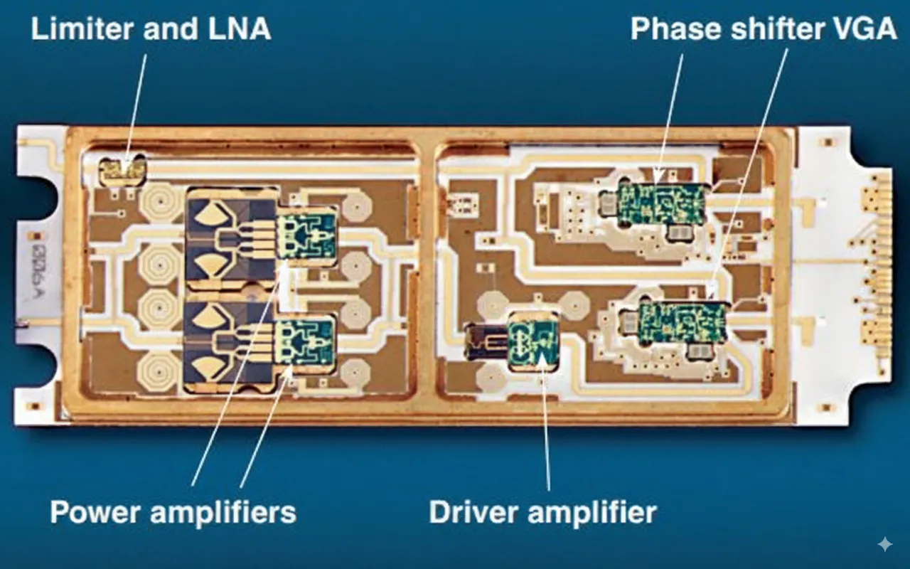
Typical T/R Module Block Diagram
A typical T/R module contains one transmit channel and one receive channel. The transmit channel generally consists of a phase shifter, a variable-gain amplifier or attenuator, a driver amplifier, and a power amplifier. Power-amplifier groups may combine several amplifiers, typically two or four, whose outputs are combined to provide the required radiating-element output power.
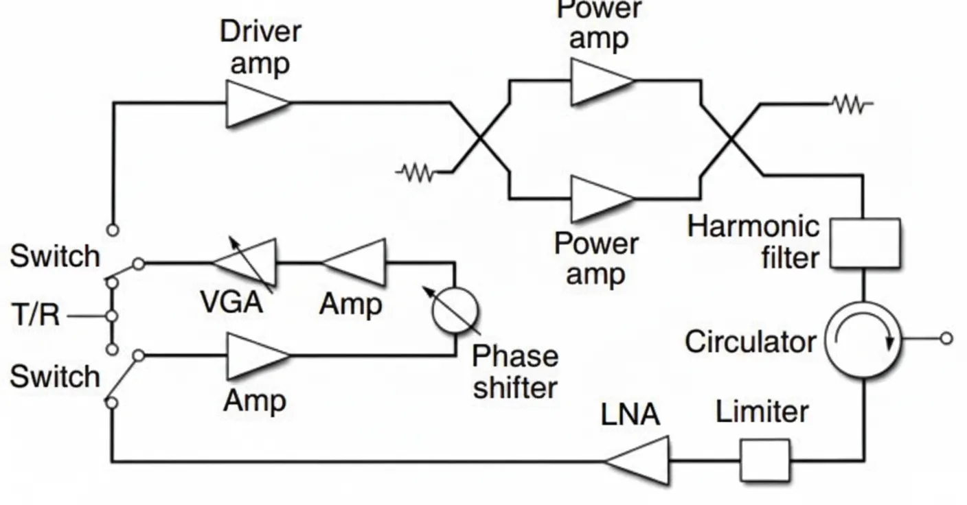
A circulator provides duplexing and isolation between the transmit and receive paths, preventing load modulation of the power amplifier caused by antenna input-impedance changes during beam scanning. The receive channel typically contains a limiter, LNA, phase shifter, and a variable-gain amplifier or attenuator. This module architecture allows designers to optimize noise figure, third-order intercept point, and dynamic range.
T/R modules commonly include voltage regulation and digital control circuitry. Local storage can preserve the transmit-pulse state to meet rise-time requirements. Series regulators adjust internal supply voltages to reduce power-supply ripple and noise to controllable levels, helping meet increasingly strict spectral-purity requirements.
Key Parameters
T/R module requirements vary by application. Important parameters include:
- Operating frequency and bandwidth
- Output power
- Power-added efficiency (PAE)
- Spurious and harmonic emissions
- Duty cycle and pulse characteristics
- Receive noise figure
- Receive gain and third-order intermodulation
- Amplitude and phase quantization
- Amplitude and phase RMS error
- Mean time between failures (MTBF)
- Cost
System function determines required frequency, bandwidth, and output power. A typical X-band T/R element is rated near 10 W and often uses commercial microwave MMICs. Lower-frequency bands typically operate at higher power. PAE is a critical metric for minimizing array power and cooling requirements; depending on technology, transmit PAE typically reaches about 20% to 25%.
LNA MMICs at microwave frequencies typically have noise figures in the 1 to 2 dB range. Accounting for losses and other effects, a module noise figure is typically 3 to 4 dB. Low-sidelobe operation requires increased phase control resolution to reduce amplitude and phase RMS errors.
Because active arrays contain many T/R modules, per-module manufacturing cost strongly affects overall affordability. Costs depend on performance, design complexity, production volume, and other factors.
Module Design and Chip Set
T/R module design must consider the number and type of integrated circuits, required output power, receive noise figure, and amplitude/phase control accuracy, as well as the radiating-element array form.
Ideally, all module circuitry would be integrated onto a single chip. For decades this has been a development goal, but differing functional requirements lead to engineering trade-offs. The common approach is to partition circuits by function, place them on separate chips, and interconnect them with hybrid microwave packaging.
A typical T/R module chip set includes several MMICs and a digital VLSI controller:
- High-power amplifier MMIC
- LNA plus protection MMIC
- Variable-gain amplifier and tunable phase shifter MMIC
- Digital control VLSI
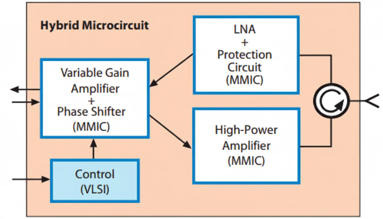
Additional circuits may be required depending on application, for example pre-driver stages to meet peak-power requirements. Most X-band and higher-frequency T/R modules currently use GaAs-based MMIC technology. GaAs has the drawback of low thermal conductivity, requiring careful thermal design. Future T/R module development trends favor GaN and SiGe processes.
GaN-based power amplifiers enable significantly higher peak power output—often more than five times that of GaAs-based circuits—improving radar sensitivity and detection range. SiGe-based implementations typically deliver less output power than GaAs but offer lower cost, making them suitable for lower-cost, lower-power-density radar systems.
Power, Efficiency, and Thermal Considerations
For a given aperture, the radar system's required average radiated power is approximately fixed. The maximum achievable average power depends on per-module output power, the number of T/R modules, module efficiency, and thermal management. With a fixed input power budget, higher module efficiency yields greater available output power.
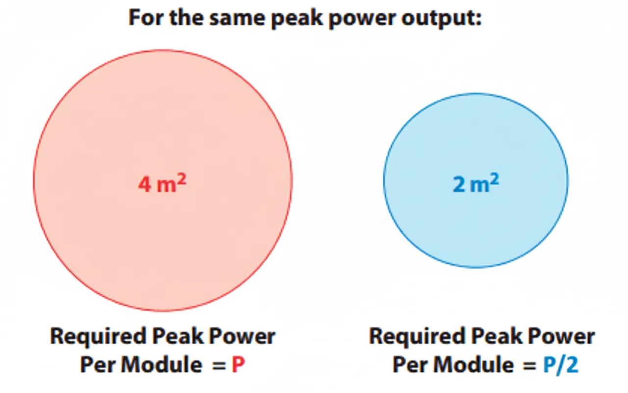
In high-power PA design, required peak power is an important metric, defined as average power divided by the minimum duty cycle. Peak power is delivered by the entire array, so once peak power is specified, the minimum number of T/R modules required is determined.
Design of radar T/R modules must take into account antenna aperture, per-module output power, and module layout. For example, to achieve the same radar detection performance with an equal number of T/R modules, each module on a 2 m2 aperture must provide twice the output power of a module on a 4 m2 aperture.
Many systems use a centralized transmitter architecture, so it is important to minimize transmitter-introduced noise. In active phased arrays, primary noise sources include DC ripple and input-voltage fluctuations. Because T/R modules operate at relatively low voltages and high currents, input-power requires appropriate filtering and regulation.
Receive Noise Figure and Amplitude/Phase Control
Receive noise figure is a critical metric for active electronically scanned array (AESA) antennas; lower receive noise figure improves radar performance. The module receive noise figure includes the LNA noise figure plus insertion loss from front-end components such as the circulator, receive protection devices, and transmission lines.
Amplitude and phase control accuracy is tied to array sidelobe requirements. If low sidelobes are required, quantization steps for amplitude and phase control must be reduced and control range increased to permit array weighting, while amplitude and phase errors must be strictly limited.
Array performance and cost depend not only on T/R modules but also on mechanical and electrical integration of the array.
Mechanical Integration and Layout
Each radiating element must be precisely positioned in the array and mounted to a rigid backplane. For systems with reduced radar cross-section requirements, array-panel deformation can increase random scattering and is difficult to correct.
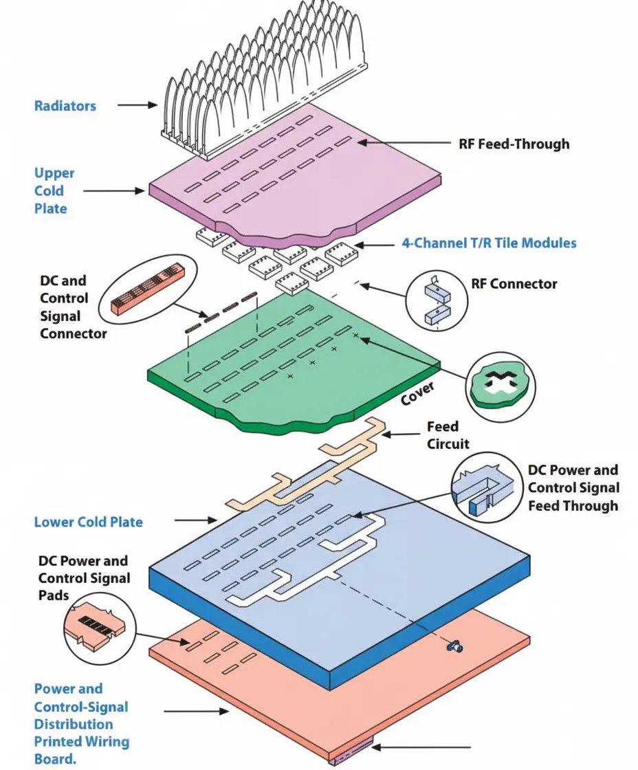
T/R modules are typically mounted to a backplane with heat-spreading structures so generated heat can be removed. Layout schemes vary; a common approach is a brick or "stick" layout.
Another approach is a tile structure. In a tile layout, modules may be formed by vertically stacking three circuit-board layers, with each layer containing multiple T/R circuits. Heat generated in module circuitry conducts through the boards to surrounding metal structures for dissipation.
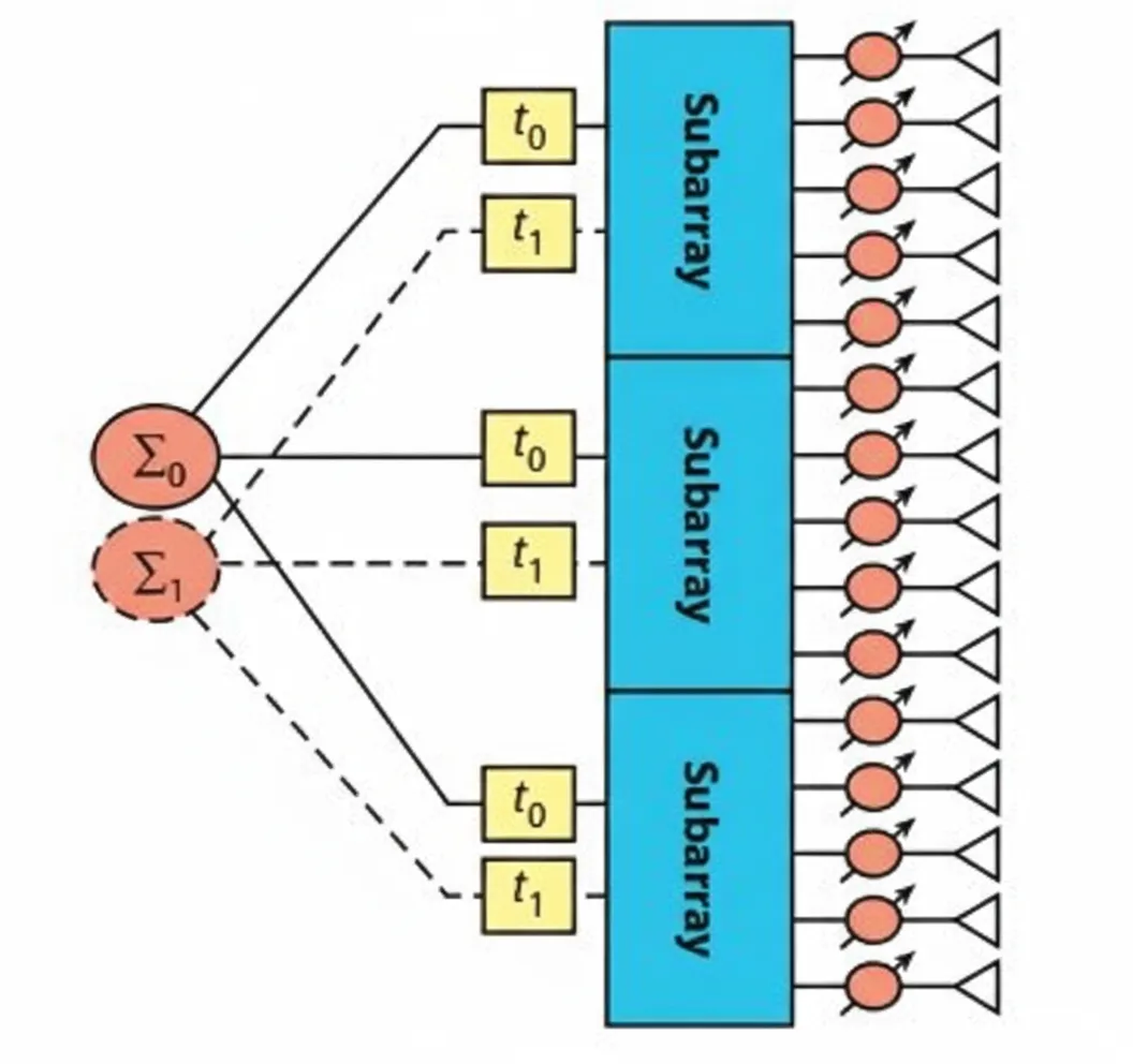
Subarray Architectures and Beamforming
Wideband or digital-beamforming systems typically use subarray-level architectures. Subarray layouts reduce manufacturing and assembly costs; analog beam scanning can be achieved by adjusting phase shifters at each subarray rear end.
In analog systems, each subarray often requires true-time-delay units to scan beams. In digital systems, the echo from each subarray is sampled directly at the receiver for digital beamforming.