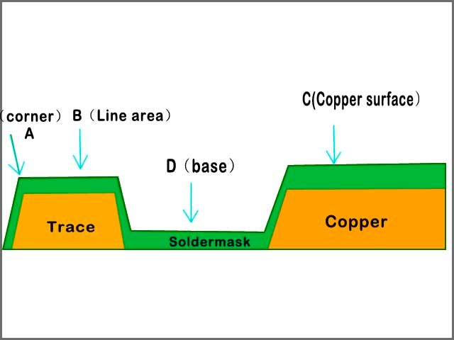
ALLPCB


In the fast-paced world of electronics design, saving space without sacrificing performance is a constant challenge. Rigid-flex PCBs offer a powerful solution, combining the stability of rigid boards with the adaptability of flexible circuits. If you're wondering how to achieve miniaturization or fit complex designs into small devices, rigid-flex PCBs are your secret weapon for space-saving innovation. In this blog, we’ll dive deep into how rigid-flex PCBs enable compact designs, support miniaturization, and often outperform traditional connectors in small devices.
What Are Rigid-Flex PCBs and Why Do They Matter for Space Saving?
Rigid-flex PCBs are hybrid circuit boards that integrate rigid and flexible sections into a single unit. The rigid parts provide structural support for components, while the flexible sections allow the board to bend or fold, fitting into tight or irregular spaces. This unique combination is a game-changer for designers working on compact devices like wearables, medical implants, or aerospace systems.
The primary advantage of rigid-flex PCBs in space saving is their ability to reduce the overall footprint of a design. Traditional rigid boards often require additional connectors or cables to link separate components, which take up valuable space. With rigid-flex technology, you eliminate the need for many of these extra parts, streamlining the design and cutting down on bulk. For example, a smartwatch design using a rigid-flex PCB can fold the flexible sections around internal components, shrinking the device’s size by up to 40% compared to using multiple rigid boards.
How Rigid-Flex PCBs Drive Miniaturization in Electronics
Miniaturization with rigid-flex PCBs is not just a trend; it’s a necessity in modern electronics. As devices get smaller—think foldable smartphones or tiny IoT sensors—engineers face the challenge of packing more functionality into less space. Rigid-flex PCBs make this possible by allowing 3D configurations. Instead of laying out components on a flat plane, designers can fold or stack the board, utilizing vertical space and reducing the device’s overall dimensions.
Consider a medical device like a wearable heart monitor. Using a rigid-flex PCB, the board can conform to the device’s curved shape, wrapping around other internal hardware. This approach can reduce the device’s thickness by as much as 30%, making it more comfortable for patients to wear. Additionally, rigid-flex designs often support higher component density, letting you place more circuits in a smaller area without compromising signal integrity. For instance, maintaining a controlled impedance of 50 ohms in high-speed applications is achievable even in tight layouts, thanks to the precise material selection in rigid-flex manufacturing.
Another key factor in miniaturization is weight reduction. Rigid-flex PCBs are lighter than assemblies of multiple rigid boards and connectors. In aerospace applications, where every gram matters, this can lead to significant savings—sometimes cutting weight by 20% or more compared to traditional designs.
Compact Rigid-Flex PCB Design: Tips for Maximum Space Efficiency
Designing a compact rigid-flex PCB requires careful planning to maximize space savings while ensuring reliability. Here are some practical tips to achieve the best results:
- Optimize Layer Stacking: Use multilayer designs to stack components vertically. A typical rigid-flex PCB might have 6-8 layers, allowing you to fit more circuitry into a smaller footprint. Ensure proper alignment between rigid and flexible sections to avoid stress points.
- Minimize Bend Radius: The flexible sections of the PCB should have a bend radius of at least 10 times the thickness of the flex material (e.g., 0.1 mm thickness requires a 1 mm bend radius) to prevent cracking or signal degradation.
- Strategic Component Placement: Place heavier components on rigid sections for stability, while using flexible areas for interconnections. This reduces mechanical stress and saves space by eliminating bulky connectors.
- Use High-Density Interconnects (HDI): Incorporate microvias and fine-pitch traces (down to 0.075 mm) to increase circuit density without expanding the board size.
By following these strategies, designers can create compact rigid-flex PCB layouts that fit into the smallest enclosures while maintaining performance. For instance, in a foldable smartphone, the hinge area often uses a flexible section to connect two rigid boards, saving up to 50% of the space that a traditional wired connection would require.
Rigid-Flex PCBs for Small Devices: Real-World Applications
Rigid-flex PCBs are ideal for small devices where space is at a premium. Let’s explore a few real-world applications where they shine:
- Wearable Technology: Devices like fitness trackers and smartwatches rely on rigid-flex PCBs to fit complex electronics into tiny, ergonomic shapes. The flexible sections can curve around batteries or displays, reducing the device’s profile by up to 35% compared to rigid-only designs.
- Medical Implants: In devices like pacemakers, rigid-flex PCBs conform to the body’s contours, minimizing size while ensuring reliability. Their ability to handle high-speed signals (up to 10 Gbps in some cases) is critical for real-time data transmission.
- Automotive Sensors: Modern vehicles use compact sensors for everything from parking assistance to engine monitoring. Rigid-flex PCBs allow these sensors to fit into tight spaces under the hood, often reducing assembly size by 25%.
These examples show how rigid-flex PCBs for small devices enable innovation across industries. Their ability to save space without compromising durability or performance makes them indispensable for cutting-edge products.
Rigid-Flex PCB vs Connectors: Which Saves More Space?
When comparing rigid-flex PCBs vs connectors, space saving is often the deciding factor. Traditional connectors, such as wire-to-board or board-to-board systems, add bulk to a design. A typical connector might occupy 5-10 mm of height and require additional clearance, whereas a rigid-flex PCB integrates connections directly into the board’s flexible sections, reducing height to under 1 mm in many cases.
Connectors also introduce points of failure. Each connection is a potential weak spot for signal loss or mechanical stress, especially in high-vibration environments like automotive or aerospace applications. Rigid-flex PCBs eliminate many of these connections, improving reliability and cutting down on space. For example, replacing a 10-pin connector with a flexible PCB section can save up to 60% of the area while maintaining signal integrity at speeds of 5 Gbps or higher.
However, connectors may still be necessary in designs requiring frequent disassembly or modular components. In such cases, a hybrid approach—using rigid-flex PCBs for internal connections and minimal connectors for external interfaces—can balance space savings with practicality.
Challenges and Considerations in Rigid-Flex PCB Design
While rigid-flex PCBs offer incredible space-saving benefits, they come with unique challenges that designers must address:
- Material Selection: Choosing the right materials for both rigid and flexible sections is critical. Polyimide is commonly used for flex areas due to its durability, but it must be paired with compatible rigid materials like FR-4 to ensure thermal stability. Mismatched materials can lead to delamination under temperature swings (e.g., -40°C to 85°C in automotive applications).
- Manufacturing Complexity: Rigid-flex PCBs require precise alignment between layers, often increasing production costs by 20-30% compared to standard rigid boards. However, the space and weight savings often justify the expense.
- Signal Integrity: High-speed designs must account for impedance mismatches in flexible sections. Maintaining a consistent 50-ohm impedance across bends requires careful trace routing and shielding, especially for signals exceeding 1 GHz.
By anticipating these challenges and collaborating with experienced manufacturing partners, designers can mitigate risks and fully leverage the space-saving potential of rigid-flex PCBs.
Why Choose Rigid-Flex PCBs for Your Next Project?
Rigid-flex PCBs are more than just a design trend—they’re a strategic choice for achieving space savings, miniaturization, and reliability in compact electronics. Whether you’re working on a wearable gadget, a medical device, or an automotive system, the ability to fold, bend, and stack components offers unmatched flexibility. Compared to traditional connectors, rigid-flex designs often save up to 50% of the space while enhancing durability and performance.
At ALLPCB, we’re committed to helping designers unlock the full potential of rigid-flex technology. Our expertise in multilayer stacking, precise material selection, and high-density interconnects ensures your compact designs meet the highest standards. By integrating rigid-flex PCBs into your workflow, you’ll not only save space but also gain a competitive edge in creating smaller, smarter, and more efficient devices.
Conclusion: Transform Your Designs with Rigid-Flex PCBs
Rigid-flex PCBs are a designer’s secret weapon for unlocking space savings and driving miniaturization in today’s compact electronics. From wearables to aerospace systems, their ability to fit into tight spaces, reduce weight, and outperform traditional connectors makes them a top choice for innovative projects. By understanding the principles of compact rigid-flex PCB design and addressing potential challenges, you can create smaller, more efficient devices that meet the demands of modern technology.
Ready to take your designs to the next level? Explore the possibilities of rigid-flex PCBs and see how they can transform your next project into a space-saving masterpiece. With the right approach and support, the future of compact electronics is within your reach.