ALLPCB


If you're looking to understand the HASL PCB manufacturing process, including molten solder, hot air leveling, PCB cleaning, and flux application, you've come to the right place. HASL, or Hot Air Solder Leveling, is a widely used surface finish technique in PCB production that ensures excellent solderability and protects copper surfaces. In this comprehensive guide, we'll walk you through every step of the HASL process, the materials involved, and the best practices to achieve optimal results. Whether you're an engineer, designer, or manufacturer, this blog will provide actionable insights to enhance your PCB projects.
What is HASL in PCB Manufacturing?
HASL stands for Hot Air Solder Leveling, a surface finish method applied to printed circuit boards (PCBs) to protect exposed copper pads and improve solderability. This process involves coating the PCB with a layer of molten solder, typically a tin-lead or lead-free alloy, and then using hot air to level the solder for a uniform finish. It’s one of the most cost-effective and reliable surface finishes, making it a popular choice for many applications.
In the sections below, we'll dive deep into the HASL PCB manufacturing process, covering everything from preparation to post-processing techniques like PCB cleaning and flux application. Let's get started with the fundamentals.
The HASL PCB Manufacturing Process: Step by Step
The HASL process is a critical part of PCB manufacturing, ensuring that the board is ready for component assembly. It requires precision and control to avoid defects like uneven solder or damaged pads. Here's a detailed breakdown of the steps involved in the HASL PCB manufacturing process.
1. Pre-Treatment and Cleaning
Before applying the solder, the PCB undergoes thorough cleaning to remove contaminants such as dust, oils, or oxidation from the copper surfaces. This step is essential to ensure proper adhesion of the molten solder. A micro-etching process is often used to create a slightly rough surface on the copper, improving solder bonding.
Pre-treatment may involve chemical cleaners or de-ionized water to achieve a pristine surface. Without proper cleaning, the solder may not adhere evenly, leading to defects during assembly.
2. Flux Application for Solderability
Flux application is a crucial step in the HASL process. Flux is a chemical agent that prevents oxidation of the copper during the high-temperature solder application and helps the molten solder flow smoothly over the pads. Typically, a rosin-based or water-soluble flux is applied to the PCB using spraying or dipping techniques.
Best practices for flux application include ensuring even coverage and using the right type of flux for the solder alloy (tin-lead or lead-free). Too much flux can leave residues, while too little may result in poor solder wetting. We'll discuss more on flux application techniques later in this guide.
3. Immersion in Molten Solder
Once the flux is applied, the PCB is dipped into a bath of molten solder at temperatures ranging from 250°C to 260°C (482°F to 500°F) for tin-lead solder, or slightly higher for lead-free alloys. This step coats the exposed copper pads with a thin layer of solder, protecting them from oxidation and preparing them for component soldering.
The duration of immersion is critical—usually just a few seconds—to avoid thermal stress on the board. The molten solder must be maintained at a consistent temperature to ensure uniform coating. Variations in temperature can lead to uneven solder thickness or incomplete coverage.
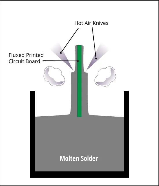
4. Hot Air Leveling for Uniform Finish
After the PCB is removed from the molten solder bath, excess solder is leveled using hot air knives. This step, known as hot air leveling, involves blowing high-pressure hot air (typically at 200°C to 250°C) across the board to remove excess solder and create a smooth, even layer. The air knives are positioned at precise angles to ensure consistency and prevent solder bridges between pads.
Hot air leveling requires advanced equipment control to avoid issues like solder stringing or uneven surfaces. The process must be carefully monitored, as improper air pressure or temperature can damage the solder mask or create defects.
5. Rapid Cooling to Solidify Solder
Once the hot air leveling is complete, the PCB is rapidly cooled to solidify the solder layer. This step is critical to forming dense and robust solder joints. If cooling is too fast, it can cause solder cracking due to thermal shock. Conversely, cooling too slowly may result in uneven solder layers. Manufacturers often use controlled cooling systems to strike the right balance.
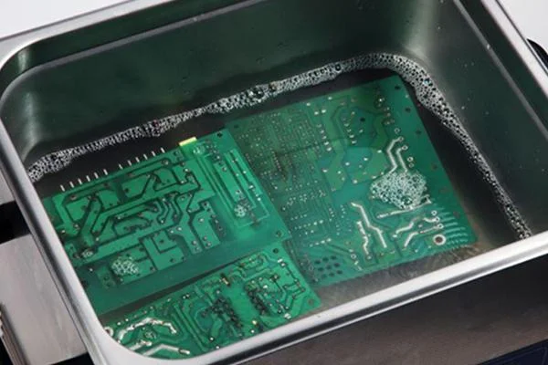
6. Post-Process PCB Cleaning
After the HASL process, residues from flux and solder may remain on the PCB surface. These residues, especially from rosin-based flux, can affect the board's reliability if not removed. PCB cleaning is performed using specialized equipment, often with de-ionized water or specific cleaning agents, to ensure a spotless surface ready for assembly.
Effective cleaning not only improves the aesthetic appearance of the PCB but also prevents long-term issues like corrosion or poor electrical performance. We'll cover best practices for PCB cleaning in more detail later.
Materials Used in the HASL Process
The quality of materials used in the HASL PCB manufacturing process directly impacts the final product's performance. Let's explore the key materials involved and their roles.
1. Solder Alloys: Tin-Lead vs. Lead-Free
Traditionally, HASL used a tin-lead alloy (typically 63% tin and 37% lead) due to its low melting point and excellent wetting properties. However, due to environmental regulations like RoHS (Restriction of Hazardous Substances), lead-free solder alloys such as SAC305 (96.5% tin, 3% silver, 0.5% copper) have become the standard in many regions.
Lead-free solders require higher processing temperatures (around 260°C to 270°C) compared to tin-lead (250°C), which can increase thermal stress on the PCB. However, they are more environmentally friendly and meet global compliance standards.
2. Flux Types and Their Importance
Flux is available in various forms, including rosin-based, water-soluble, and no-clean options. Rosin flux is widely used in HASL due to its excellent ability to prevent oxidation, but it often leaves sticky residues that require thorough cleaning. Water-soluble flux is easier to clean but may be more corrosive if not removed properly. No-clean flux minimizes post-process cleaning but may not be suitable for all applications.
Choosing the right flux depends on the specific requirements of your PCB project, including the solder type and assembly process.
3. PCB Substrate and Copper Quality
The base material of the PCB, often FR-4 or other laminates, must withstand the high temperatures of the HASL process without warping or delaminating. Additionally, the copper layer's purity and thickness (typically 1 oz or 2 oz per square foot) play a role in how well the solder adheres. High-quality copper ensures better solderability and reduces the risk of defects.
Advantages and Limitations of HASL
Understanding the benefits and drawbacks of HASL helps in deciding if it’s the right surface finish for your project. Here's a quick overview.
Advantages of HASL
- Cost-Effective: HASL is one of the most affordable surface finishes, making it ideal for budget-conscious projects.
- Excellent Solderability: The solder coating ensures strong joints during component assembly.
- Long Shelf Life: HASL-finished PCBs resist oxidation, maintaining solderability over extended periods.
Limitations of HASL
- Uneven Surface: Hot air leveling can sometimes result in uneven solder thickness, which may not be suitable for fine-pitch components.
- Thermal Stress: The high temperatures involved can stress the PCB, potentially causing warping in thinner boards.
- Not Ideal for HDI: High-density interconnect (HDI) designs may require flatter finishes like ENIG due to HASL's inconsistent surface.
Best Practices for HASL PCB Manufacturing
To achieve the best results with HASL, manufacturers must follow certain best practices across the process. Below are actionable tips for optimizing each stage, focusing on molten solder, hot air leveling, PCB cleaning, and flux application.
1. Optimizing Flux Application Techniques
Flux application must be precise to ensure proper solder wetting without excessive residue. Use automated spraying systems for uniform coverage, especially on complex board designs. Monitor the flux concentration regularly, as degradation can affect performance. For rosin-based flux, ensure the cleaning process is robust to remove all residues.
Additionally, store flux in controlled conditions to prevent contamination or evaporation, which can alter its effectiveness. Always match the flux type to the solder alloy for compatibility.
2. Controlling Molten Solder Temperature
Maintain a stable temperature for the molten solder bath to ensure consistent coating. For tin-lead solder, keep the temperature between 250°C and 260°C, while lead-free alloys may require 260°C to 270°C. Use high-quality solder with minimal impurities to prevent dross formation, which can lead to uneven coatings.
Regularly test the solder bath composition, as contamination over time can degrade quality. Replace or purify the solder as needed to maintain performance.
3. Precision in Hot Air Leveling
During hot air leveling, adjust the air knife pressure and temperature based on the board's design and solder type. Typical air temperatures range from 200°C to 250°C, with pressure settings fine-tuned to avoid solder bridges. Modern equipment often includes sensors to monitor and adjust these parameters in real-time, reducing defects.
Ensure the air knives are clean and free of debris, as blockages can disrupt airflow and cause uneven leveling. Regular maintenance of the equipment is essential for consistent results.
4. Effective PCB Cleaning Methods
Post-HASL PCB cleaning is non-negotiable for reliability. Use ultrasonic cleaning systems with de-ionized water or specialized solvents to remove flux residues. For rosin-based flux, a saponifier solution can help break down sticky residues. Ensure the cleaning process doesn't damage the solder mask or components by controlling water pressure and temperature.
Dry the PCB thoroughly after cleaning to prevent moisture-related issues. Automated drying systems with warm air can speed up this process while ensuring no water spots remain.
Applications of HASL in PCB Projects
HASL is suitable for a wide range of applications due to its cost-effectiveness and reliability. It's commonly used in consumer electronics, industrial control systems, and automotive electronics where fine-pitch components are not a primary concern. For projects requiring high-density designs or ultra-flat surfaces, alternative finishes may be considered, but HASL remains a go-to choice for many standard applications.
For example, in power supply boards, HASL provides robust solder joints that withstand high currents and thermal cycling. Its ability to maintain solderability over time also makes it ideal for products with long storage periods before assembly.
Conclusion: Mastering HASL for Superior PCB Results
The HASL PCB manufacturing process, with its use of molten solder, hot air leveling, precise flux application, and thorough PCB cleaning, is a proven method for achieving reliable and cost-effective surface finishes. By understanding each step—from pre-treatment to cooling—and following best practices, manufacturers can minimize defects and ensure high-quality PCBs ready for assembly.
Whether you're working on a simple prototype or a large-scale production run, HASL offers a balance of performance and affordability. Keep the tips and techniques shared in this guide in mind to optimize your process, focusing on temperature control, equipment precision, and post-process cleaning. With the right approach, HASL can be a powerful tool in your PCB manufacturing toolkit.