 ALLPCB


In the world of electronics design, PCB trace routing and complex PCB layouts are critical to ensuring your circuits perform at their best. Whether you're working on high-speed digital designs or intricate multilayer boards, navigating the challenges of signal trace management and routing for signal integrity can make or break your project. In this comprehensive guide, we'll dive deep into the realities of routing complex layouts, explore effective autorouting strategies, and provide actionable tips to optimize your PCB designs for maximum performance.
Why PCB Trace Routing Matters in Complex Layouts
PCB trace routing is the process of creating conductive pathways on a printed circuit board to connect components. In simple designs, routing might be straightforward, but in complex PCB layouts, it becomes a puzzle of balancing space, signal integrity, and electrical performance. Poor routing can lead to issues like signal interference, crosstalk, or even complete circuit failure. For engineers tackling high-density or high-speed designs, mastering trace routing is essential to ensure reliable operation.
Key Challenges in Routing Complex PCB Layouts
Designing a PCB with maximum components and intricate connections comes with several hurdles. Let's break down the main challenges and how they impact signal trace management.
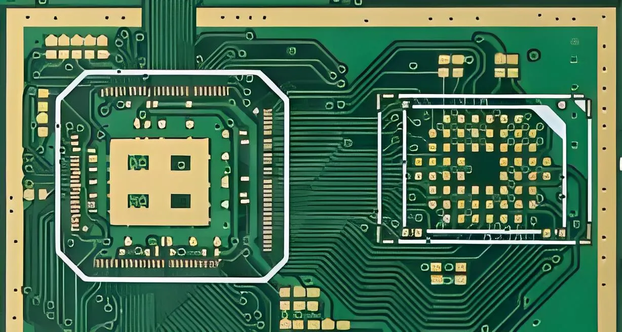
1. Limited Space and High Component Density
In modern electronics, devices are getting smaller, but the number of components keeps growing. This creates a high-density layout where every millimeter counts. Routing traces in such tight spaces often means dealing with overlapping paths or insufficient clearance between traces, which can lead to electrical shorts or interference.
2. Signal Integrity at High Speeds
High-speed signals, such as those in USB 3.0 (operating at 5 Gbps) or DDR4 memory (up to 3.2 GHz), are highly sensitive to trace length, impedance mismatch, and crosstalk. Without proper routing for signal integrity, these signals can degrade, causing data errors or system crashes.
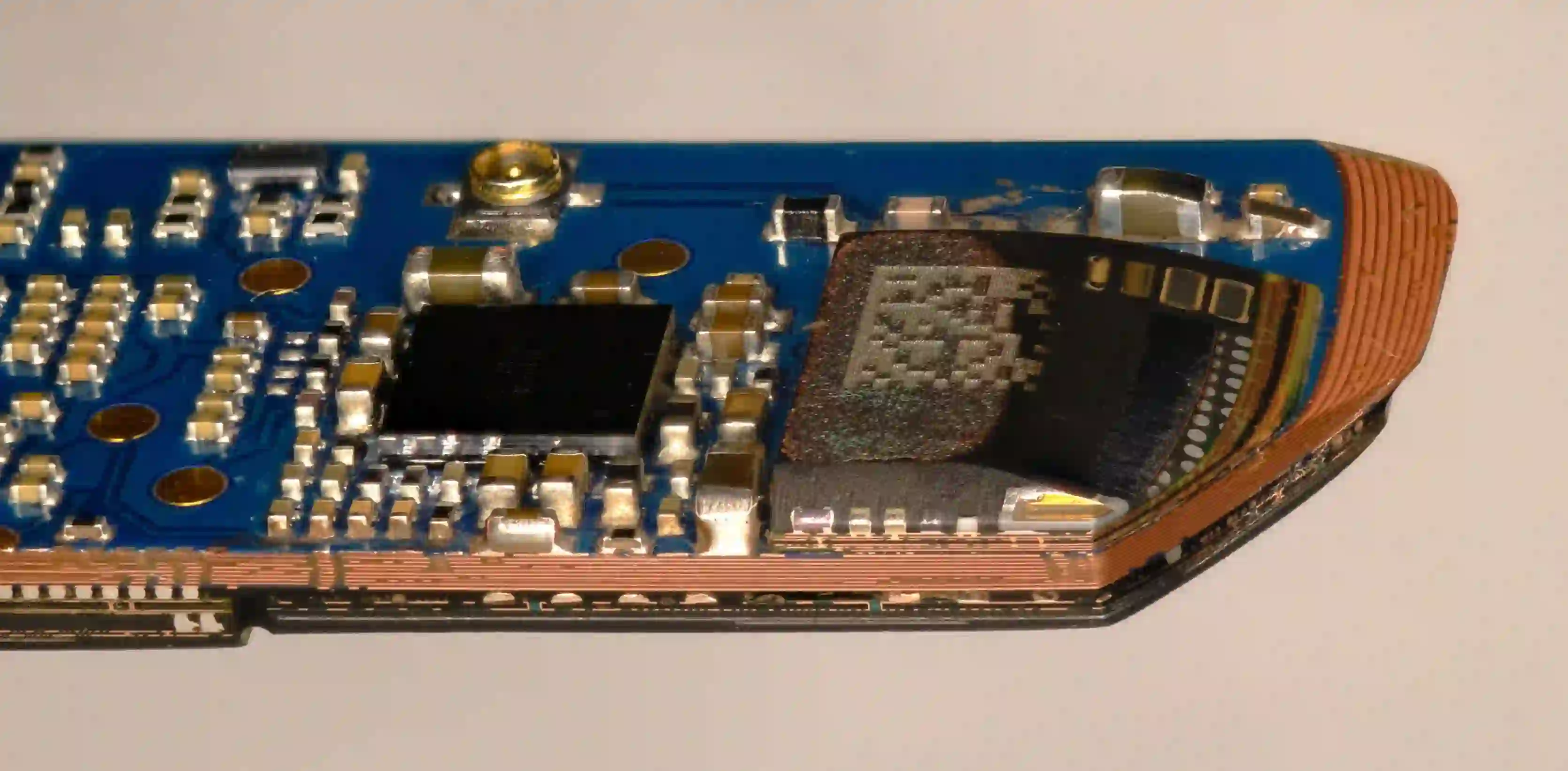
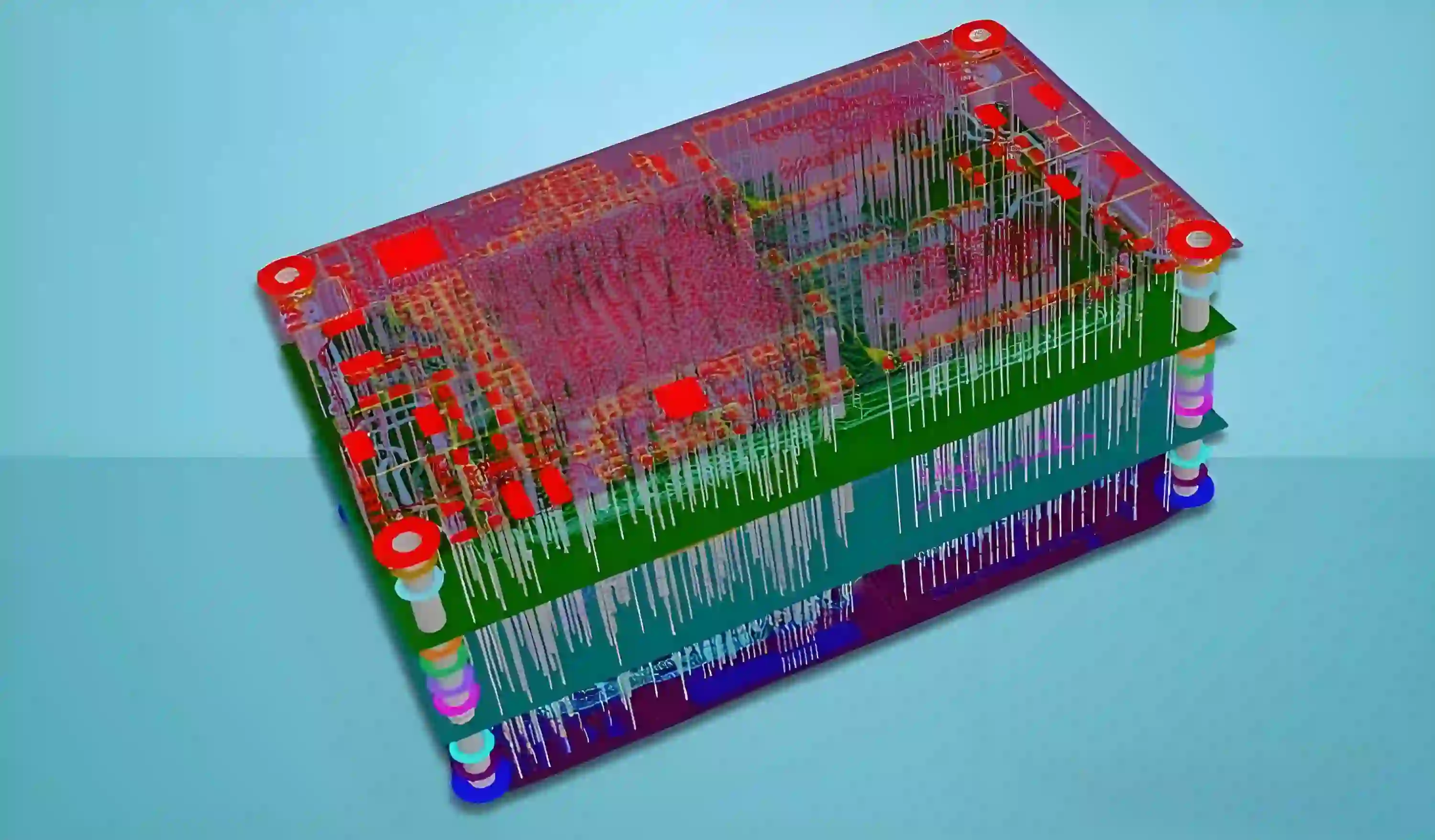
3. Multilayer Complexity
Many complex designs require multilayer boards—sometimes 8, 12, or even 16 layers—to accommodate all the traces and components. Routing across multiple layers adds complexity, as engineers must manage vias (connections between layers) and ensure signals don't interfere with each other.
Essential Strategies for Effective PCB Trace Routing
Navigating complex PCB layouts requires a strategic approach. Below are proven strategies to optimize your routing process and maintain signal integrity.
1. Prioritize Critical Nets First
Start by routing the most critical signals, such as high-speed data lines or power traces. These nets often have strict requirements for length matching or impedance control. For instance, in a design with differential pairs (common in USB or Ethernet), traces must be routed with equal lengths to avoid timing skews—differences as small as 0.1 mm can cause signal delays at high frequencies.
2. Maintain Proper Trace Width and Spacing
Trace width and spacing directly affect impedance and crosstalk. For a 50-ohm impedance (common in RF designs), trace width might need to be around 6-10 mils (0.15-0.25 mm) depending on the board material and layer stackup. Spacing between traces should be at least 3 times the trace width to minimize crosstalk. Use impedance calculators or simulation tools to determine exact values for your design.
3. Use Ground Planes for Shielding
A solid ground plane beneath signal traces acts as a shield, reducing electromagnetic interference (EMI) and improving routing for signal integrity. Ensure the ground plane is unbroken under high-speed traces to avoid signal return path disruptions.
4. Minimize Via Usage in High-Speed Paths
Vias introduce inductance and capacitance, which can distort high-speed signals. When routing across layers, try to keep vias to a minimum, and if unavoidable, use microvias or blind vias for better performance.
Autorouting Strategies: Boon or Bane for Complex Layouts?
Autorouting strategies are often seen as a time-saver, especially in complex PCB layouts with hundreds or thousands of connections. However, while autorouting tools can handle basic designs, they often fall short in intricate projects. Here's how to use autorouting effectively and when to avoid it.
Benefits of Autorouting
Autorouting can quickly generate trace paths for non-critical nets, saving hours of manual work. It's particularly useful for power and ground connections in early design stages, allowing engineers to focus on critical signals.
Limitations and Pitfalls
Autorouting tools lack the nuanced understanding of signal priorities or design constraints. They may create inefficient paths, ignore impedance requirements, or place vias in problematic areas. For instance, an autorouted high-speed trace might take a longer, meandering path, introducing delays or interference.
Best Practice: Hybrid Approach
The best way to leverage autorouting strategies is to combine them with manual routing. Use autorouting for low-priority nets after manually routing critical signals. Always review and adjust autorouted traces to ensure they meet design rules and performance goals.
Signal Trace Management for Optimal Performance
Effective signal trace management is the cornerstone of a successful PCB design. Here are key techniques to keep your signals clean and reliable.
1. Length Matching for Differential Pairs
In high-speed designs, differential pairs (like those in PCIe or HDMI) must have matched trace lengths to ensure signals arrive simultaneously. A mismatch of even 5 mils (0.127 mm) can cause timing issues at frequencies above 1 GHz. Use serpentine routing to add small bends and match lengths precisely.
2. Avoid Sharp Corners
Sharp 90-degree corners in traces can cause signal reflections due to impedance discontinuities. Instead, use 45-degree angles or rounded corners to maintain signal flow, especially for frequencies above 100 MHz.
3. Separate Analog and Digital Signals
Analog and digital signals can interfere with each other if routed too closely. Keep them on separate layers or areas of the board, and use ground planes or guard traces to isolate sensitive analog signals.
Routing for Signal Integrity: Best Practices
Routing for signal integrity is about minimizing noise, interference, and signal loss. Here are actionable best practices to follow.
1. Control Impedance with Stackup Design
Impedance control starts with the PCB stackup. For a 50-ohm trace on a standard FR-4 material (dielectric constant of 4.5), the trace width and distance to the ground plane must be carefully calculated. A typical 4-layer board might have signal layers on top and bottom, with ground and power planes in the middle for shielding.
2. Reduce Crosstalk with Proper Spacing
Crosstalk occurs when signals on adjacent traces interfere. Maintain a spacing of at least 3 times the trace width for high-speed signals. For very sensitive designs, increase this to 5 times the width or add guard traces connected to ground between signal lines.
3. Use Decoupling Capacitors Near ICs
Place decoupling capacitors (e.g., 0.1 μF ceramic capacitors) close to integrated circuits to filter out noise on power lines. Route power traces to these capacitors first before connecting to the IC pins to ensure a clean supply.
Tools and Techniques for Mastering Complex PCB Layouts
Modern PCB design software offers powerful features to tackle complex PCB layouts. Features like interactive routing, design rule checks (DRC), and signal integrity simulation help engineers visualize and optimize trace paths. Additionally, simulation tools can predict issues like crosstalk or impedance mismatch before fabrication, saving time and cost.
For multilayer boards, layer stackup planners are invaluable. They allow you to define the arrangement of signal, ground, and power layers to minimize interference. Always run a final DRC to ensure no spacing or clearance violations exist in your design.
Common Mistakes to Avoid in PCB Trace Routing
Even experienced engineers can make mistakes when routing complex PCB layouts. Here are some pitfalls to watch out for:
- Ignoring Design Rules: Failing to set or follow design rules for trace width, spacing, or via size can lead to manufacturing issues or signal problems.
- Over-Reliance on Autorouting: As discussed earlier, autorouting can't replace manual oversight for critical nets.
- Poor Grounding: Incomplete or improperly placed ground planes can create return path issues, leading to EMI and noise.
- Neglecting Thermal Management: High-current traces need wider paths to handle heat dissipation—overlooking this can cause board damage.
Conclusion: Mastering Routing for Maximum PCB Performance
Routing traces on a PCB is both an art and a science, especially when dealing with complex PCB layouts. By prioritizing critical signals, leveraging smart autorouting strategies, and focusing on signal trace management, you can create designs that perform reliably under any conditions. Remember that routing for signal integrity is not just about connecting points—it's about ensuring every signal travels cleanly and efficiently.
Whether you're designing a high-speed digital board or a densely packed IoT device, the principles of effective PCB trace routing remain the same: plan meticulously, route strategically, and verify thoroughly. With these tips and techniques, you're well-equipped to tackle even the most challenging layouts and achieve maximum performance in your PCB designs.


