 ALLPCB


In the world of high-speed electronics, maintaining signal integrity in multilayer printed circuit boards (PCBs) is crucial for performance and reliability. If you're working with a 14-layer PCB, you might be wondering how to optimize signal integrity to ensure your design operates without errors or interference. The answer lies in careful planning, precise impedance control, effective layer stacking, and advanced simulation tools. In this comprehensive guide, we'll dive deep into the best practices for achieving top-notch signal integrity in 14-layer PCB designs, covering everything from high-speed PCB design principles to reducing crosstalk and using signal integrity simulation.
Why Signal Integrity Matters in 14-Layer PCBs
Signal integrity refers to the quality of an electrical signal as it travels through a PCB. In high-speed designs, even small distortions can lead to data errors, timing issues, or complete system failure. A 14-layer PCB, often used in complex applications like telecommunications, aerospace, and advanced computing, has multiple signal, power, and ground layers. While this complexity allows for greater functionality, it also increases the risk of interference, crosstalk, and impedance mismatches.
Optimizing 14-layer PCB signal integrity ensures that signals remain clear and reliable, even at high frequencies (often above 1 GHz). Poor signal integrity can result in costly redesigns or product failures, making it a top priority for engineers working on multilayer boards.
Understanding the Basics of 14-Layer PCB Design
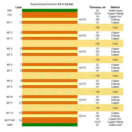
A 14-layer PCB typically consists of alternating signal, power, and ground layers. This stackup is designed to minimize electromagnetic interference (EMI) and provide stable power distribution. For high-speed applications, a common configuration might include:
- 4 to 6 signal layers for routing high-speed traces.
- Multiple ground planes to reduce noise and provide a return path for signals.
- Power planes to ensure consistent voltage delivery across the board.
The exact arrangement depends on the specific requirements of your design, but the goal remains the same: to create a balanced structure that supports high-speed PCB design while maintaining signal integrity.
Key Challenges in 14-Layer PCB Signal Integrity
Before diving into optimization techniques, let’s look at the main challenges you’ll face:
- Crosstalk: Unwanted coupling of signals between adjacent traces or layers, especially in dense designs.
- Impedance Mismatches: Variations in trace impedance can cause signal reflections and degrade performance.
- Signal Delay: Longer trace lengths or improper routing can introduce timing issues in high-speed circuits.
- EMI: High-frequency signals can radiate or pick up interference, affecting nearby components.
Addressing these challenges requires a combination of design strategies, material selection, and simulation tools tailored for multilayer boards.
Strategies for Optimizing Signal Integrity in 14-Layer PCBs
Let’s explore actionable techniques to ensure optimal performance in your 14-layer PCB design. These strategies focus on impedance control in multilayer PCBs, routing practices, and layer stackup optimization.
1. Design an Effective Layer Stackup
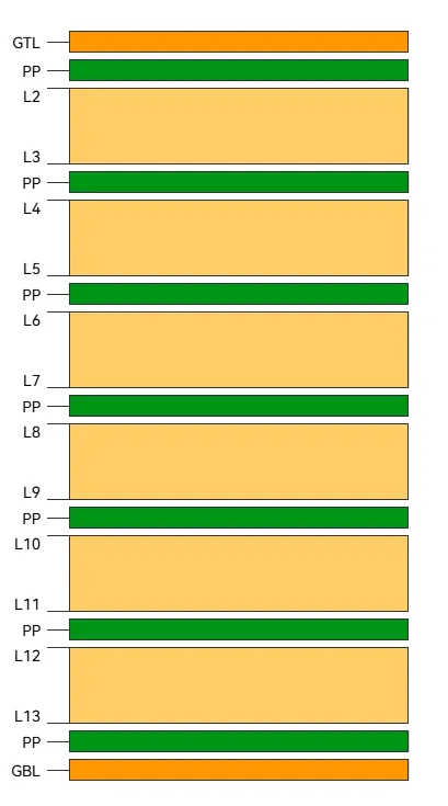
The foundation of signal integrity lies in the layer stackup. For a 14-layer PCB, a well-planned stackup minimizes noise and provides a stable reference for high-speed signals. A typical stackup might look like this:
- Layer 1: Top Signal (High-Speed Traces)
- Layer 2: Ground Plane
- Layer 3: Signal
- Layer 4: Power Plane
- Layer 5: Ground Plane
- Layer 6: Signal
- Layer 7: Power Plane
- Layer 8: Ground Plane
- Layer 9: Signal
- Layer 10: Power Plane
- Layer 11: Ground Plane
- Layer 12: Signal
- Layer 13: Ground Plane
- Layer 14: Bottom Signal
This configuration ensures that each signal layer is adjacent to a ground or power plane, providing a consistent return path and reducing EMI. Keep high-speed signals on outer layers or layers close to ground planes to minimize interference.
2. Implement Impedance Control in Multilayer PCBs
Impedance control is critical for maintaining signal integrity in high-speed designs. In a 14-layer PCB, traces carrying high-speed signals must have a consistent characteristic impedance, often 50 ohms for single-ended signals or 100 ohms for differential pairs.
To achieve impedance control in multilayer PCBs, follow these steps:
- Calculate Trace Width and Spacing: Use an impedance calculator to determine the correct trace width and spacing based on the dielectric constant (Dk) of your PCB material (typically 3.5 to 4.5 for FR-4) and the target impedance.
- Choose the Right Material: Select low-loss materials with stable dielectric properties for high-frequency applications. Materials with a Dk of around 3.2 and a dissipation factor (Df) below 0.005 are ideal for frequencies above 5 GHz.
- Maintain Uniform Layer Thickness: Ensure consistent dielectric thickness between signal layers and reference planes to avoid impedance variations.
By maintaining controlled impedance, you can prevent signal reflections that degrade performance in high-speed circuits.
3. Minimize Crosstalk in High-Speed Designs
Crosstalk occurs when signals on adjacent traces or layers interfere with each other, a common issue in dense 14-layer PCBs. Reducing crosstalk in PCBs is essential for maintaining clear signals. Here are some proven techniques:
- Increase Trace Spacing: Keep high-speed traces at least 3 times the trace width apart to reduce coupling. For differential pairs, maintain consistent spacing between the pair while keeping them away from other signals.
- Use Ground Planes: Place ground planes between signal layers to shield traces from interference. This is especially effective in a 14-layer design where multiple ground planes can be incorporated.
- Route Signals on Different Layers: Avoid running high-speed signals parallel to each other on the same layer for long distances. If necessary, route them on separate layers with a ground plane in between.
- Minimize Via Usage: Vias can introduce noise and crosstalk. Use back-drilling for high-speed vias to remove unused stub sections, reducing signal distortion.
Implementing these practices can significantly lower crosstalk and improve overall signal quality.
4. Optimize Routing for High-Speed PCB Design
Routing plays a major role in high-speed PCB design. Poor routing can introduce delays, reflections, and noise. Follow these guidelines for effective routing in a 14-layer PCB:
- Keep Traces Short and Direct: Minimize trace length for high-speed signals to reduce propagation delay. Aim for trace lengths under 1/10th of the wavelength of the highest frequency signal (e.g., for a 5 GHz signal, keep traces under 6 mm if possible).
- Avoid Sharp Corners: Use 45-degree angles or curved traces instead of 90-degree bends to prevent signal reflections.
- Match Trace Lengths: For differential pairs or parallel data buses, match trace lengths to within 5 mils (0.127 mm) to avoid timing skew.
- Route Over Ground Planes: Ensure high-speed traces are routed over continuous ground planes to provide a low-impedance return path.
Proper routing ensures signals arrive at their destination without distortion or delay, a key factor in high-speed applications.
5. Leverage Signal Integrity Simulation Tools
Designing a 14-layer PCB for high-speed applications is complex, and manual calculations alone may not catch all issues. This is where signal integrity simulation comes in. Simulation tools allow you to model your design and predict potential problems before manufacturing.
Key aspects of signal integrity simulation include:
- Impedance Analysis: Simulate trace impedance to ensure it matches the target value (e.g., 50 ohms) across all high-speed lines.
- Crosstalk Evaluation: Identify areas where crosstalk might occur and adjust trace spacing or layer assignments accordingly.
- Eye Diagram Testing: Use eye diagrams to assess signal quality at the receiver end. A clear, open eye indicates good signal integrity, while a closed or distorted eye suggests issues like jitter or noise.
- Reflection Analysis: Detect and mitigate signal reflections caused by impedance mismatches or improper terminations.
By incorporating simulation into your workflow, you can catch and fix issues early, saving time and cost during the prototyping phase.
Material Selection for High-Speed 14-Layer PCBs
The choice of materials impacts signal integrity, especially at high frequencies. Standard FR-4 materials may suffice for lower-speed designs, but high-speed 14-layer PCBs often require advanced laminates with better electrical properties.
- Low-Loss Dielectrics: Materials like Rogers 4350B or Isola 370HR offer a lower dielectric constant (around 3.3) and reduced loss tangent (below 0.004), ideal for frequencies above 2 GHz.
- Consistent Dk and Df: Ensure the material’s dielectric constant and dissipation factor remain stable across the operating temperature range to avoid impedance variations.
- Thin Dielectrics: Use thinner dielectric layers (e.g., 5 mils or 0.127 mm) between signal and ground planes to achieve tighter impedance control.
Selecting the right material is a balancing act between performance and cost, but for high-speed designs, investing in premium materials often pays off in improved reliability.
Power Integrity and Its Role in Signal Integrity
Signal integrity isn’t just about signal traces; it’s also closely tied to power integrity. In a 14-layer PCB, power planes must deliver stable voltage to all components without introducing noise. Poor power distribution can cause voltage drops or ripples that affect signal quality.
To optimize power integrity:
- Use Multiple Power Planes: Dedicate separate layers to different voltage levels (e.g., 3.3V, 1.8V) to avoid interference.
- Place Decoupling Capacitors: Position capacitors close to power pins of high-speed ICs to filter out noise. Use a mix of values (e.g., 0.1 μF and 1 μF) to cover a wide frequency range.
- Minimize Power Plane Splits: Avoid splitting power planes under high-speed traces, as this disrupts the return path and introduces noise.
A stable power supply enhances signal integrity by ensuring consistent performance across the board.
Conclusion: Achieving Excellence in 14-Layer PCB Design
Optimizing 14-layer PCB signal integrity is a multifaceted process that requires attention to layer stackup, impedance control, routing, and simulation. By implementing the strategies outlined in this guide—such as designing an effective stackup, maintaining impedance control in multilayer PCBs, reducing crosstalk in PCBs, and leveraging signal integrity simulation—you can ensure your high-speed designs perform reliably even in the most demanding applications.
Whether you’re working on telecommunications equipment, advanced computing systems, or other complex electronics, a focus on high-speed PCB design principles will set your project up for success. With careful planning and the right tools, you can overcome the challenges of multilayer PCB design and deliver products that meet the highest standards of performance and reliability.
At ALLPCB, we’re committed to supporting engineers with resources and expertise to bring their designs to life. By following these best practices, you’ll be well on your way to mastering signal integrity in your next 14-layer PCB project.


