ALLPCB


If you're looking to master HDI PCB reflow soldering and ensure HDI PCB solder joint reliability, you're in the right place. High-Density Interconnect (HDI) PCBs are critical in modern electronics, packing more components into smaller spaces. However, their complex designs demand precise soldering techniques to avoid failures. In this guide, we'll walk you through the best practices for the HDI PCB soldering process, focusing on achieving strong, reliable joints that stand the test of time.
At ALLPCB, we understand the challenges of working with intricate HDI designs. This blog will cover everything from preparing your board to optimizing reflow profiles, inspecting joints, and troubleshooting common issues. Let’s dive into the details to help you achieve top-quality results.
What is HDI PCB Reflow Soldering?
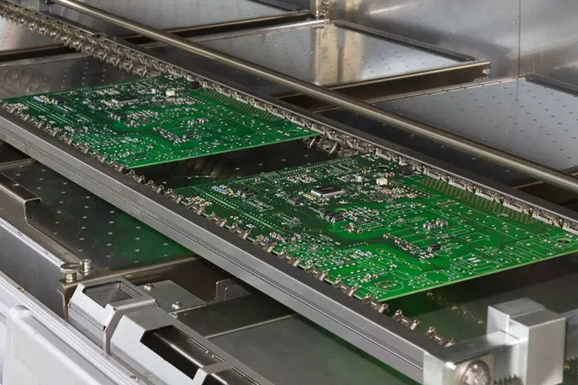
HDI PCBs are designed with finer lines, smaller vias, and denser component layouts compared to traditional PCBs. These characteristics make the HDI PCB soldering process more challenging. Reflow soldering, a widely used method in surface-mount technology (SMT), involves applying solder paste to the board, placing components, and heating the assembly in a controlled oven to melt the solder and form strong joints.
For HDI PCBs, the process requires extra precision due to tighter tolerances and smaller pad sizes. A single misstep can lead to weak joints, thermal stress, or component damage. Understanding the nuances of HDI PCB reflow soldering is key to ensuring reliability and performance in applications like smartphones, medical devices, and automotive electronics.
Why Solder Joint Reliability Matters for HDI PCBs
HDI PCB solder joint reliability directly impacts the functionality and lifespan of electronic devices. Poor joints can result in intermittent connections, signal loss, or complete failure, especially in high-stakes applications where reliability is non-negotiable. For instance, in automotive systems, a failed solder joint could disrupt critical sensors operating at high temperatures or vibrations.
Reliable joints ensure proper electrical conductivity and mechanical strength. With HDI PCBs often featuring microvias and fine-pitch components, even minor defects like voids or cracks can cause significant issues. By following best practices in the HDI PCB soldering process, you can minimize risks and enhance durability.
Best Practices for HDI PCB Reflow Soldering
Let’s break down the essential steps and techniques to achieve flawless results in HDI PCB reflow soldering. These practices are designed to address the unique challenges of HDI designs and ensure consistent, reliable outcomes.
1. Proper Board and Component Preparation
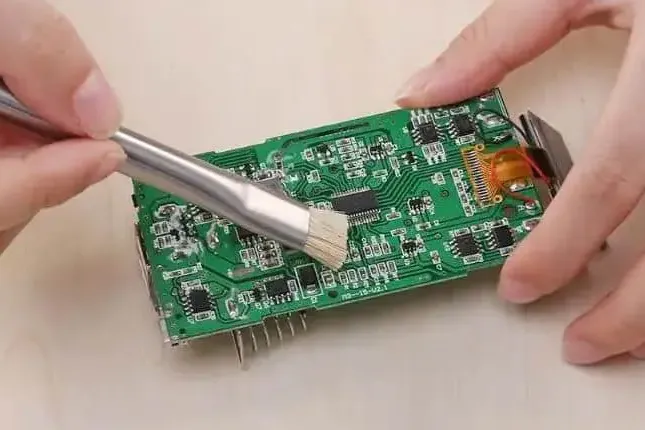
Preparation is the foundation of a successful HDI PCB soldering process. Start by ensuring your PCB and components are clean and free from contaminants like dust, oil, or oxidation. Even tiny impurities can prevent proper solder wetting, leading to weak joints.
- Clean the PCB: Use isopropyl alcohol and a lint-free cloth to clean the board surface. For stubborn residues, consider ultrasonic cleaning.
- Inspect Components: Check for bent pins or damaged leads on fine-pitch components. HDI designs often use small packages like 0201 or 01005, which are prone to misalignment.
- Solder Paste Storage: Store solder paste at the recommended temperature (typically 2-10°C) and allow it to reach room temperature before use to avoid condensation.
2. Precise Solder Paste Application
Solder paste application is critical for HDI PCB solder joint reliability. HDI boards often have pad sizes as small as 0.2 mm, requiring exact amounts of paste to avoid excess or insufficient solder.
- Use a High-Quality Stencil: Opt for laser-cut stencils with a thickness of 0.1-0.15 mm for fine-pitch components. Ensure the stencil apertures match the pad sizes to prevent bridging or insufficient paste.
- Control Paste Volume: Apply just enough paste to cover 80-90% of the pad area after reflow. Over-application can cause solder balls, while under-application leads to weak joints.
- Choose the Right Paste: Use a lead-free solder paste with a Type 4 or Type 5 particle size for HDI applications. These finer particles ensure better deposition on small pads.
3. Component Placement with Precision
In HDI designs, components are placed closer together, often with spacing as tight as 0.3 mm. Misplacement can lead to shorts or open circuits during reflow.
- Use Automated Placement Machines: Manual placement is impractical for HDI PCBs. Automated pick-and-place machines ensure accuracy within ±0.01 mm.
- Verify Alignment: Double-check component orientation and alignment before reflow, especially for fine-pitch ICs and BGAs (Ball Grid Arrays).
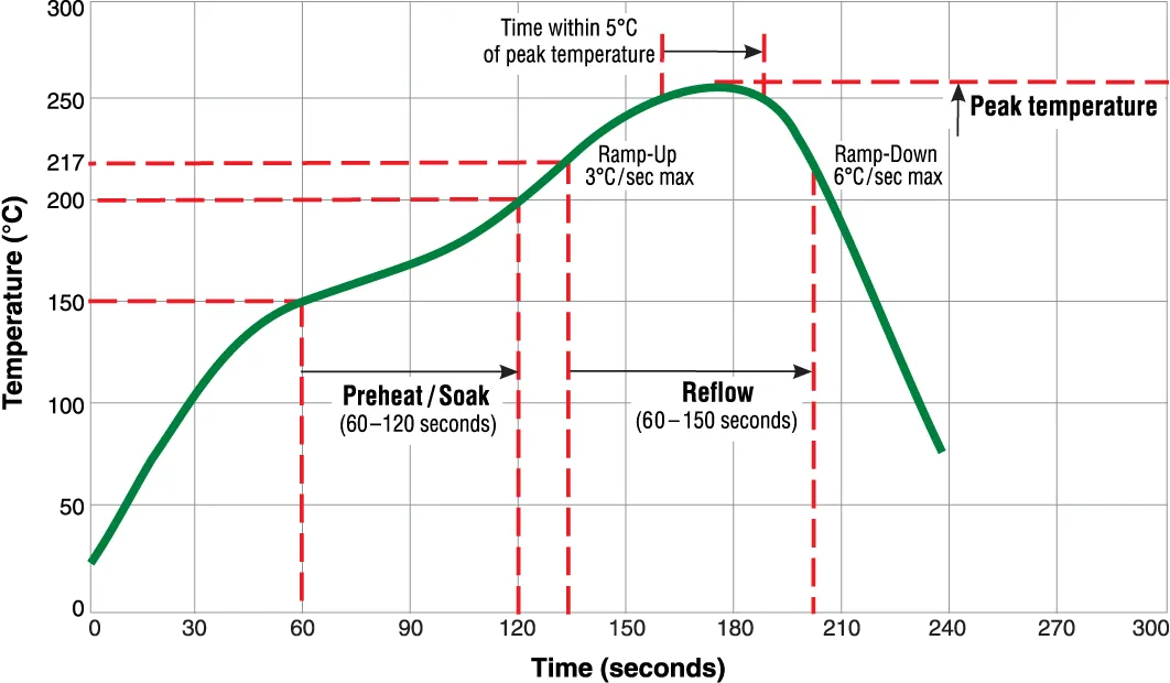
4. Optimize the Reflow Temperature Profile
The reflow temperature profile is the heart of the HDI PCB reflow soldering process. A well-designed profile ensures the solder paste melts, wets the pads, and forms strong joints without damaging components or the board.
- Preheat Zone (50-150°C): Gradually heat the board over 60-120 seconds to evaporate solvents in the solder paste and prevent thermal shock. A ramp rate of 1-3°C per second is ideal.
- Soak Zone (150-200°C): Maintain this temperature for 60-90 seconds to activate the flux and ensure uniform heating across the dense HDI layout.
- Reflow Zone (220-250°C for lead-free solder): Peak temperature should be 20-40°C above the solder’s melting point (typically 217°C for SAC305 alloy) for 20-40 seconds. Avoid exceeding component manufacturer limits, often around 260°C.
- Cooling Zone: Cool the board at a rate of 2-4°C per second to solidify the solder joints without inducing thermal stress.
For HDI PCBs with varying component sizes, consider a custom profile to balance heat distribution. Larger components may require slightly longer soak times to ensure even heating.
5. Use Nitrogen Atmosphere if Needed
For HDI PCBs with ultra-fine features, soldering in a nitrogen atmosphere can improve HDI PCB solder joint reliability. Nitrogen reduces oxidation during reflow, leading to better wetting and fewer defects like voids.
- Target Oxygen Levels: Keep oxygen levels below 100 ppm in the reflow oven for optimal results.
- Cost Consideration: While nitrogen reflow adds cost, it’s worth it for high-reliability applications like aerospace or medical devices.
6. Post-Reflow Inspection and Testing
After reflow, inspecting the solder joints is crucial to confirm the success of the HDI PCB soldering process. HDI designs make visual inspection challenging, so advanced tools are often necessary.
- Automated Optical Inspection (AOI): Use AOI systems to detect issues like bridging, insufficient solder, or misalignment on fine-pitch components.
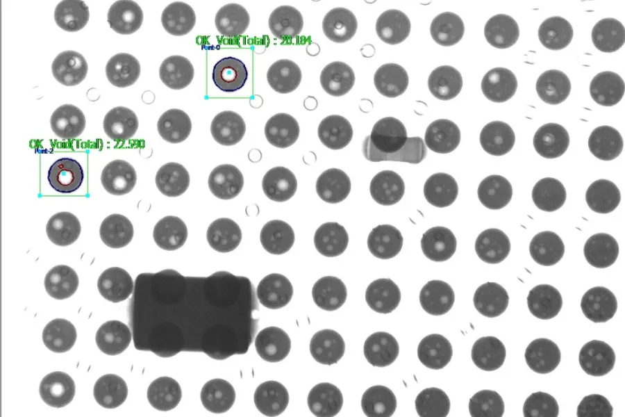
- X-Ray Inspection: For BGAs and other hidden joints, X-ray imaging reveals voids or cracks. Aim for void percentages below 25% of the joint area for reliability.
- Electrical Testing: Perform in-circuit testing to verify connectivity and signal integrity, especially for high-speed HDI designs operating at frequencies above 1 GHz.
Common Challenges in HDI PCB Reflow Soldering and Solutions
Even with the best preparation, challenges can arise during HDI PCB reflow soldering. Here are some common issues and how to address them for improved HDI PCB solder joint reliability.
1. Tombstoning of Small Components
Tombstoning occurs when small components (like 0201 resistors) stand upright due to uneven heating or solder wetting. This is common in HDI designs with mixed component sizes.
- Solution: Ensure uniform pad design and paste application. Adjust the reflow profile to slow down the ramp rate in the preheat zone to below 2°C per second.
2. Solder Voids in BGAs
Voids are air pockets in solder joints that weaken mechanical and thermal performance, a frequent issue in HDI PCBs with BGAs.
- Solution: Use a longer soak time (90-120 seconds) to allow outgassing of flux volatiles. Consider vacuum reflow ovens for critical applications to minimize voids below 10%.
3. Thermal Stress and Warpage
HDI PCBs often use thinner substrates (0.6-1.0 mm), making them prone to warpage under high reflow temperatures.
- Solution: Use fixtures or carriers to support the board during reflow. Optimize the cooling rate to prevent sudden temperature drops that cause stress.
Advanced Tips for Enhancing Solder Joint Reliability
For engineers aiming to push the boundaries of HDI PCB solder joint reliability, consider these advanced strategies:
- Profile Simulation: Use thermal profiling software to simulate heat distribution across the HDI PCB. This helps identify hot or cold spots before actual production.
- Solder Alloy Selection: Beyond standard SAC305, explore low-temperature alloys (melting at 138-170°C) for heat-sensitive components in HDI designs.
- Conformal Coating: After soldering, apply a conformal coating to protect joints from moisture and vibration, especially for HDI PCBs in harsh environments.
Why Choose ALLPCB for Your HDI PCB Needs?
At ALLPCB, we specialize in delivering high-quality HDI PCB solutions tailored to your project requirements. Our state-of-the-art manufacturing and assembly processes ensure precision in every step of the HDI PCB soldering process. Whether you need support with fine-pitch components, custom reflow profiles, or rigorous quality testing, our team is ready to assist.
We prioritize HDI PCB solder joint reliability by adhering to strict industry standards and using cutting-edge inspection tools. Partner with us to bring your complex designs to life with confidence.
Conclusion
Mastering HDI PCB reflow soldering is essential for creating reliable, high-performance electronics. By following the best practices outlined in this guide—from meticulous preparation to optimized reflow profiles and thorough inspection—you can achieve exceptional HDI PCB solder joint reliability. The HDI PCB soldering process may be complex, but with the right techniques, you can overcome challenges and ensure long-lasting results.