 ALLPCB


Scaling from a prototype to full-scale production for smart home device PCB manufacturing can be a complex journey. Whether you're designing a smart thermostat, a connected security camera, or a voice-activated assistant, the process involves navigating challenges like cost efficiency, supply chain management, and assembly hurdles. In this comprehensive guide, we’ll walk you through the essential steps of the PCB manufacturing process, strategies for scaling PCB production, and solutions to common obstacles, ensuring a smooth transition to market-ready products.
At ALLPCB, we understand the intricacies of bringing innovative smart home devices to life. This blog will dive deep into actionable insights on cost-effective PCB manufacturing, overcoming PCB assembly challenges, and optimizing supply chain management for PCBs. Let’s explore how to turn your prototype into a production success.
Understanding the PCB Manufacturing Process for Smart Home Devices
The PCB manufacturing process is the foundation of any smart home device. These devices often require compact, high-performance boards to handle sensors, connectivity modules, and power management systems. Here's a breakdown of the key stages in creating a PCB, tailored to the needs of smart home technology.
1. Design and Prototyping: The journey begins with designing the PCB layout using specialized software. For smart home devices, the design must accommodate components like Wi-Fi modules, microcontrollers, and power regulators, often within tight space constraints. Once the design is finalized, a prototype is created to test functionality. This stage often involves multiple iterations to refine signal integrity—ensuring, for example, that high-speed data lines maintain impedance values around 50 ohms for optimal performance.
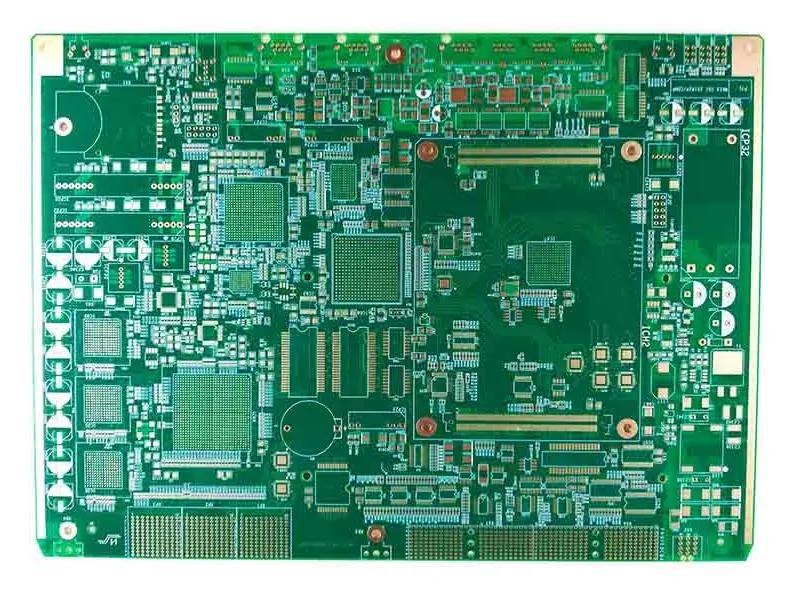
2. Fabrication: After validating the prototype, the design files are sent for fabrication. This process includes etching copper layers, drilling vias (with diameters as small as 0.2 mm for high-density boards), and applying solder masks. For smart home devices, multi-layer PCBs are common to support complex circuitry, often requiring 4 to 8 layers.
3. Assembly: During assembly, components are mounted onto the board using surface-mount technology (SMT) or through-hole methods. Precision is critical, as components for smart home devices, like tiny 0402 resistors or QFN packages, demand placement accuracy within 0.1 mm to avoid connection issues.
4. Testing and Quality Control: Rigorous testing ensures the PCB functions as intended. For smart home devices, this includes checking wireless signal strength (often targeting -85 dBm or better for reliable connectivity) and power consumption (aiming for standby currents below 1 mA to extend battery life). Automated optical inspection (AOI) and in-circuit testing (ICT) are often used to detect defects.
Scaling PCB Production: Key Strategies for Success
Transitioning from a few prototypes to mass production is where scaling PCB production becomes critical. For smart home devices, which often target consumer markets with high demand, scaling must balance quality, speed, and cost. Here are proven strategies to achieve this.
1. Optimize Design for Manufacturability (DFM): Before scaling, revisit your PCB design to ensure it’s optimized for production. This means minimizing the number of unique components to reduce inventory complexity and using standard sizes (e.g., 0603 capacitors instead of custom sizes) to lower costs. DFM can cut production expenses by up to 20% by reducing assembly errors and material waste.
2. Partner with Reliable Manufacturers: Collaborating with a trusted PCB provider ensures access to advanced equipment and expertise. Look for capabilities like high-volume SMT lines that can handle 50,000 placements per hour, ensuring scalability without bottlenecks.
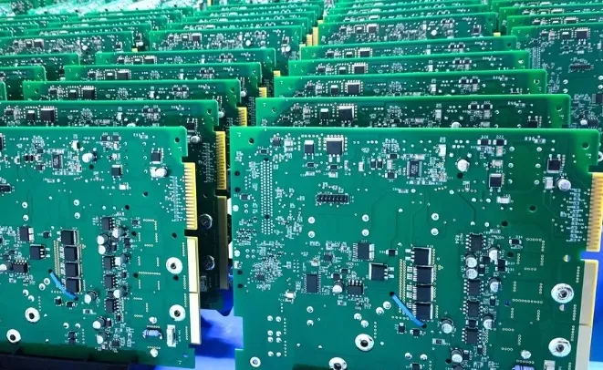
3. Plan for Volume Increases: Start with small batch runs (e.g., 500-1,000 units) to identify potential issues before committing to larger orders of 10,000 units or more. Gradually increasing volume helps manage risks, especially for smart home devices where firmware updates or hardware tweaks might be needed post-launch.
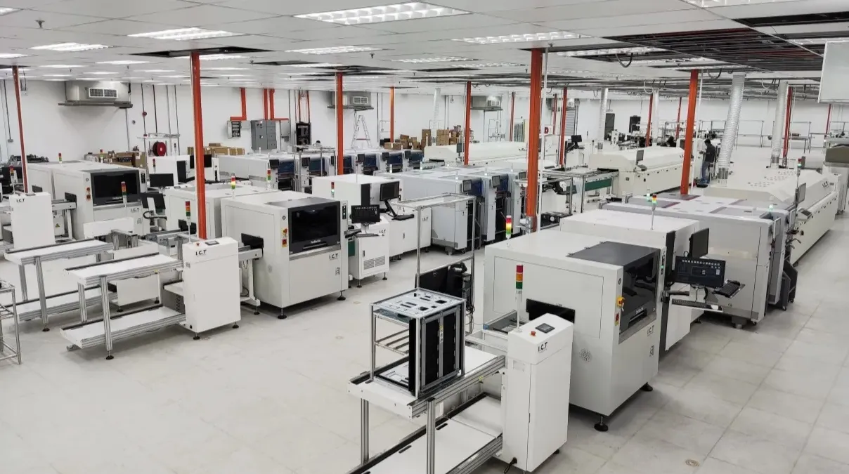
4. Leverage Automation: Automated assembly and testing processes are essential for scaling. Modern pick-and-place machines can achieve speeds of 100,000 components per hour, drastically reducing labor costs and human error in high-volume production.
PCB Assembly Challenges and How to Overcome Them
PCB assembly challenges often arise when scaling production for smart home devices. These devices require precision and reliability to meet consumer expectations. Below are common hurdles and practical solutions.
1. Component Miniaturization: Smart home devices often use tiny components to save space, such as 0201 resistors or BGA chips with 0.4 mm pitch. Misalignment during assembly can lead to shorts or open circuits. Solution: Invest in high-precision assembly equipment and use X-ray inspection to verify solder joints under BGAs, ensuring defect rates stay below 0.1%.
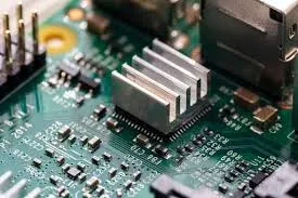
2. Thermal Management: High-performance components like processors in smart hubs generate heat, risking board failure if not managed. Solution: Incorporate thermal vias and heat sinks in the design, targeting a maximum operating temperature of 85°C for critical components.
3. Signal Integrity Issues: With high-speed signals in Wi-Fi and Bluetooth modules, crosstalk and electromagnetic interference (EMI) can degrade performance. Solution: Use controlled impedance traces (typically 50 ohms for RF signals) and proper grounding planes to maintain signal integrity, achieving data rates up to 2.4 Gbps for wireless communication.
4. Component Shortages: Global supply disruptions can delay assembly due to unavailable parts like specific microcontrollers. Solution: Design with alternative components in mind (e.g., pin-compatible substitutes) and maintain buffer stock for critical parts to cover at least 2-3 months of production.
Cost-Effective PCB Manufacturing: Balancing Quality and Budget
Cost-effective PCB manufacturing is a priority when scaling production for smart home devices. With consumer markets often demanding competitive pricing, keeping expenses low without sacrificing quality is essential. Here’s how to achieve this balance.
1. Material Selection: Choose cost-efficient materials that meet performance needs. For instance, FR-4 substrates are widely used for their affordability and reliability in standard smart home applications, costing around $0.10 per square inch for basic boards, compared to $0.50 for high-frequency materials.
2. Reduce Layer Count: While multi-layer boards are common, reducing layers from 6 to 4 can lower fabrication costs by 15-20% without compromising functionality for simpler devices like smart plugs.
3. Bulk Ordering: Ordering components and PCBs in larger quantities often yields discounts. For example, purchasing 10,000 resistors at once can reduce per-unit costs by up to 30% compared to small batches of 100.
4. Minimize Rework: Defects during assembly lead to costly rework. Implementing strict quality controls, such as AOI systems that detect 99.9% of placement errors, can save thousands in repair costs over a production run of 50,000 units.
Supply Chain Management for PCBs: Ensuring Smooth Scaling
Effective supply chain management for PCBs is crucial to avoid delays and cost overruns when scaling production. Smart home device manufacturers often face global supply chain disruptions, making strategic planning vital. Here are key considerations.
1. Source Diversification: Relying on a single supplier for critical components like capacitors or ICs can halt production if shortages occur. Maintain relationships with at least two suppliers per part to reduce risk, ensuring a backup if lead times extend beyond the typical 8-12 weeks for semiconductors.
2. Inventory Management: Use just-in-time (JIT) inventory practices to minimize storage costs while keeping buffer stock for high-demand parts. For instance, maintaining a 4-week supply of Wi-Fi modules can prevent production stops during unexpected delays.
3. Logistics Optimization: Shipping costs and delays can impact budgets. Partner with logistics providers offering consolidated shipping options to cut costs by up to 25% compared to individual shipments, especially for international component sourcing.
4. Real-Time Tracking: Leverage supply chain software to monitor component availability and shipping statuses. This can reduce lead time uncertainties by providing alerts when delays are likely, allowing for proactive adjustments.
Industry Trends Impacting Smart Home PCB Manufacturing
The smart home industry is evolving rapidly, and staying ahead requires adapting to emerging trends during PCB manufacturing and scaling. Here are two key trends to consider.
1. IoT Integration: With global IoT device shipments projected to exceed 75 billion by 2025, smart home PCBs must support advanced connectivity like Zigbee, Z-Wave, and 5G. Designs should prioritize low-power protocols, targeting current draws under 10 μA in sleep mode for battery-powered devices.
2. Sustainability: Consumers and regulators are pushing for eco-friendly products. Use lead-free solder and recyclable materials in PCB production to meet standards like RoHS, reducing environmental impact while appealing to green-conscious markets.
Conclusion: Partnering for Success in Smart Home PCB Manufacturing
Scaling from prototype to production for smart home device PCB manufacturing is a multi-faceted process that demands attention to design, assembly, cost, and supply chain logistics. By optimizing the PCB manufacturing process, addressing assembly challenges, and implementing cost-effective strategies, you can bring innovative products to market efficiently. Strong supply chain management for PCBs further ensures that production runs smoothly, even amidst global disruptions.
At ALLPCB, we’re committed to supporting your journey with end-to-end solutions for scaling PCB production. From high-precision fabrication to streamlined assembly, our expertise helps overcome obstacles and deliver quality smart home devices to your customers. Start transforming your prototypes into market-ready products with confidence today.


