 ALLPCB


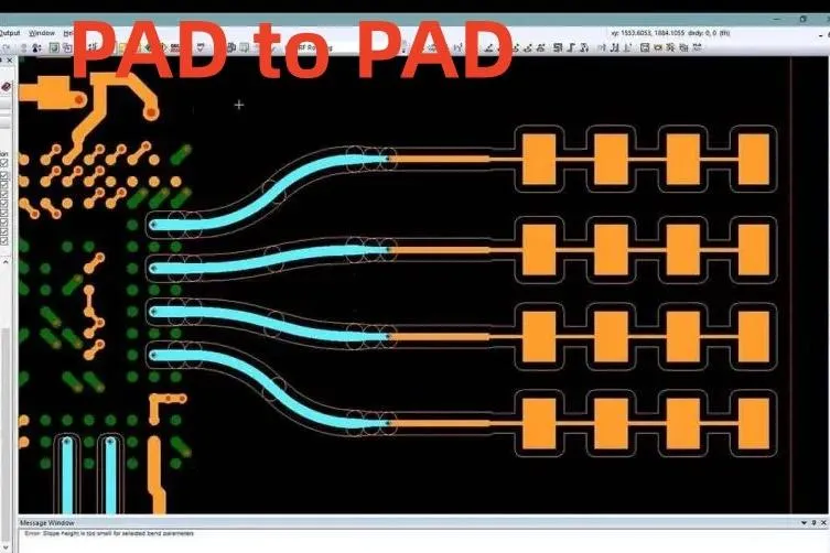
In the world of PCB design, achieving high-speed signal integrity is a top priority, especially as devices become faster and more compact. One often overlooked factor that plays a critical role in maintaining signal quality is pad-to-pad spacing. So, how does pad spacing impact high-speed designs? Simply put, proper pad-to-pad spacing minimizes crosstalk, controls impedance, and ensures reliable data transmission in high-speed circuits. In this detailed guide, we’ll dive deep into the importance of pad spacing for PCB signal integrity, explore high-speed design rules, and uncover strategies for crosstalk minimization and differential pair routing.
Why Pad-to-Pad Spacing Matters in High-Speed PCB Design
High-speed PCB design is all about ensuring that signals travel from one point to another without distortion or interference. Pad-to-pad spacing—the distance between the conductive pads on a PCB—directly influences how signals behave. If pads are too close, you risk unwanted electrical coupling, also known as crosstalk, which can degrade signal quality. If they’re too far apart, it can affect the board’s layout efficiency and potentially alter impedance characteristics.
In high-speed designs, where signals can operate at frequencies above 100 MHz, even tiny variations in spacing can lead to significant issues. For instance, improper spacing might cause a signal’s impedance to deviate from the standard 50 ohms or 100 ohms (common for differential pairs), leading to reflections and data errors. Let’s break down the key aspects of why pad spacing is a cornerstone of PCB signal integrity.
The Basics of Signal Integrity in High-Speed Designs
Signal integrity refers to the quality of an electrical signal as it travels through a PCB. In high-speed applications, such as USB, HDMI, or Ethernet interfaces, maintaining signal integrity is crucial for reliable performance. Factors like impedance mismatch, crosstalk, and signal delay can all disrupt data transmission. Pad-to-pad spacing impacts these factors by influencing how much electromagnetic interference (EMI) occurs between adjacent pads and traces.
How Pad Spacing Impacts Impedance in High-Speed Designs
Impedance control is a fundamental principle in high-speed design rules. It ensures that signals travel along traces without reflections, which can distort data. The pad spacing impact on impedance is significant because the spacing between pads affects the capacitance and inductance of the signal path. When pads are too close, the capacitance increases, lowering the impedance. This mismatch can cause signal reflections, especially in high-speed circuits operating at 1 GHz or higher.
For example, in a typical 50-ohm single-ended trace, if the pad spacing is reduced below the recommended value (often around 0.2 mm for fine-pitch components), the impedance might drop to 45 ohms or lower, leading to signal loss. To avoid this, designers must adhere to spacing guidelines based on the dielectric constant of the PCB material (commonly 4.2 for FR-4) and the target impedance. Using simulation tools to model these effects before manufacturing can save time and prevent costly redesigns.
Practical Tips for Impedance Control with Pad Spacing
- Follow manufacturer guidelines for minimum pad spacing, typically ranging from 0.15 mm to 0.3 mm for high-speed components.
- Use a consistent dielectric material thickness (e.g., 0.1 mm to 0.2 mm for inner layers) to maintain uniform impedance across the board.
- Route critical traces over a continuous ground plane to reduce impedance variations caused by pad proximity.
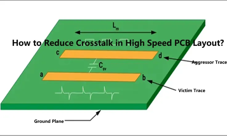
Crosstalk Minimization: The Role of Pad-to-Pad Spacing
Crosstalk is the unwanted transfer of energy between adjacent signals, and it’s a major concern in high-speed designs. When pads are placed too closely, the electromagnetic fields around them can couple, causing interference. This is especially problematic in dense layouts where multiple high-speed signals run parallel to each other. Effective crosstalk minimization starts with optimizing pad-to-pad spacing.
For instance, a spacing of less than 0.1 mm between pads in a high-speed design can result in crosstalk levels exceeding -20 dB, which is enough to corrupt data in protocols like USB 3.0 (operating at 5 Gbps). To combat this, designers often increase spacing to at least three times the trace width or use ground vias between pads to shield signals. This approach creates a barrier that absorbs stray electromagnetic energy, reducing interference.
Strategies for Crosstalk Reduction
- Maintain a pad-to-pad spacing of at least 0.2 mm for high-speed signals to minimize coupling.
- Place ground pads or vias strategically between high-speed signal pads to act as a shield.
- Avoid routing high-speed traces parallel to each other for long distances near pads; instead, stagger them to reduce coupling.
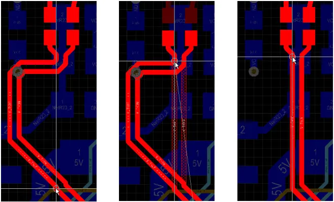
Differential Pair Routing and Pad Spacing Considerations
Differential pair routing is a common technique in high-speed designs to transmit data with minimal noise. Used in standards like USB, Ethernet, and PCIe, differential pairs consist of two traces carrying equal and opposite signals. The receiver reads the difference between these signals, canceling out common-mode noise. However, pad spacing plays a crucial role in maintaining the balance of these pairs.
If the pads for a differential pair are unevenly spaced or too close to other signals, it can introduce skew—where one signal arrives slightly before the other. Even a small skew of 10 picoseconds can cause errors in a 10 Gbps signal. To prevent this, the pad spacing for differential pairs should be symmetric and match the trace spacing (often around 0.1 mm to 0.15 mm for a 100-ohm differential impedance). Additionally, the pads must be placed away from other high-speed signals to avoid crosstalk.
Best Practices for Differential Pair Pad Spacing
- Ensure equal spacing between the pads of a differential pair to maintain signal balance.
- Keep differential pair pads at least 0.3 mm away from other signal pads to prevent interference.
- Use a continuous ground plane under differential pair pads to stabilize impedance and reduce EMI.
High-Speed Design Rules: Balancing Pad Spacing with Layout Constraints
While optimizing pad-to-pad spacing is essential for high-speed design rules, it must be balanced with the overall layout constraints of the PCB. Modern devices often require dense component placement, leaving little room for generous spacing. This is where careful planning and simulation come into play. Designers must prioritize critical signals—such as clock lines or data buses—by allocating more spacing to their pads while using shielding techniques for less critical areas.
For example, in a multi-layer PCB with a 1.6 mm thickness, you might allocate 0.25 mm spacing for high-speed signal pads on the top layer while reducing spacing to 0.15 mm for lower-speed signals on inner layers. Additionally, using automated design rule checks (DRC) in your PCB software can help identify spacing violations before fabrication, ensuring compliance with industry standards like IPC-2221.
Key High-Speed Design Rules for Pad Spacing
- Adhere to minimum spacing rules based on signal speed; for signals above 1 GHz, aim for 0.2 mm or more between pads.
- Group high-speed signal pads away from power and ground pads to avoid noise coupling.
- Use simulation tools to analyze the electromagnetic field distribution around pads and adjust spacing accordingly.
Common Challenges and Solutions in Pad Spacing for High-Speed Designs
Designing for high-speed signal integrity often comes with challenges related to pad spacing. One common issue is the trade-off between spacing and board size. Increasing spacing to reduce crosstalk can lead to larger boards, which may not be feasible for compact devices. To address this, designers can use advanced PCB materials with lower dielectric constants (e.g., below 3.5), which reduce capacitance and allow for tighter spacing without sacrificing signal integrity.
Another challenge is maintaining consistent spacing in fine-pitch components like BGAs (Ball Grid Arrays), where pad spacing can be as tight as 0.4 mm. In such cases, using microvias and high-density interconnect (HDI) technology can help route signals away from crowded areas, preserving signal quality.
Tools and Techniques for Optimizing Pad Spacing
Modern PCB design software offers powerful tools to help engineers optimize pad-to-pad spacing for high-speed applications. Features like impedance calculators, signal integrity simulators, and automated spacing checks allow designers to predict and resolve issues before manufacturing. For instance, running a pre-layout simulation can reveal whether a 0.15 mm pad spacing will cause excessive crosstalk at 2.5 GHz, enabling adjustments early in the design process.
Additionally, collaborating with your PCB fabrication partner can provide valuable insights into achievable spacing based on their manufacturing capabilities. Some fabricators may support spacing as tight as 0.1 mm with advanced processes, while others may require a minimum of 0.2 mm for reliable production.
Conclusion: Mastering Pad Spacing for Superior Signal Integrity
Pad-to-pad spacing is a small but mighty factor in achieving high-speed signal integrity. By carefully controlling spacing, designers can mitigate issues like impedance mismatch, crosstalk, and signal skew, ensuring reliable performance in even the fastest circuits. Whether you’re working on differential pair routing, adhering to high-speed design rules, or focusing on crosstalk minimization, understanding the pad spacing impact on impedance is key to success.
At ALLPCB, we’re committed to helping you navigate the complexities of PCB signal integrity. By applying the guidelines and strategies discussed in this post, you can design boards that meet the demands of today’s high-speed technologies. Remember to leverage simulation tools, prioritize critical signals, and balance spacing with layout constraints for the best results. With the right approach, cracking the code of pad-to-pad spacing becomes a powerful tool in your PCB design arsenal.


