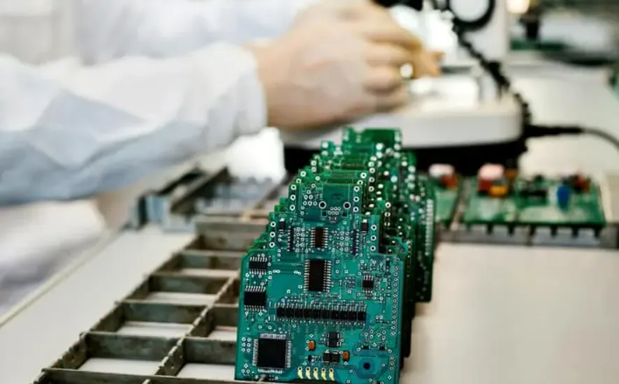
ALLPCB


In the world of high-speed PCB design, maintaining signal integrity is a constant battle. Two key players in this fight are backdrilling and via stubs. So, which one wins in combating signal degradation? Backdrilling often takes the lead by physically removing unused via stubs, reducing signal reflections, and minimizing crosstalk in PCBs. Via stubs, if left unaddressed, can act as unwanted antennas, causing signal loss and interference. In this comprehensive guide, we’ll dive deep into the differences between backdrilling and via stubs, explore signal integrity issues, and provide actionable insights on reducing signal reflections and crosstalk for optimal PCB performance.
Introduction: Why Signal Integrity Matters in PCB Design
As electronic devices push the boundaries of speed and performance, signal integrity has become a critical factor in PCB design. High-speed signals, often running at frequencies above 1 GHz, are prone to degradation due to reflections, crosstalk, and impedance mismatches. These issues can lead to data errors, slower performance, and even complete system failures. Two common challenges in multilayer PCB designs are via stubs and their effects on signal quality. Backdrilling emerges as a powerful technique to address these problems, but how does it compare to leaving via stubs in place? Let’s explore the fundamentals of via stubs, the role of backdrilling, and practical strategies for winning the war against signal degradation.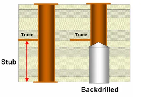
What Are Via Stubs and Their Effects on Signal Integrity?
In multilayer PCBs, vias are small conductive pathways that connect different layers of the board. When a via extends beyond the layer where the signal is routed, the unused portion is called a via stub. While this stub might seem harmless, it can wreak havoc on high-speed signals. Here’s how via stub effects manifest as signal integrity issues:
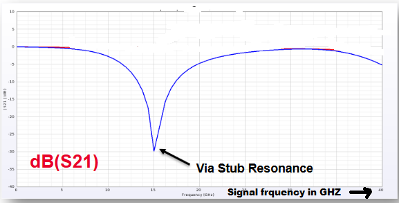
- Signal Reflections: Via stubs act like unterminated transmission lines, causing signal reflections. These reflections bounce back and interfere with the original signal, leading to distortion. For instance, at frequencies above 2 GHz, a stub as short as 0.5 mm can cause noticeable reflection losses.
- Signal Attenuation: The stub absorbs part of the signal energy, reducing its amplitude. This attenuation can degrade data transfer rates, especially in applications like DDR4 memory, where signal margins are tight.
- Resonance and Jitter: Via stubs can resonate at specific frequencies, introducing deterministic jitter. This jitter disrupts timing accuracy, critical for high-speed digital systems operating at 10 Gbps or higher.
- Crosstalk: Stubs can couple with nearby vias or traces, increasing electromagnetic interference (EMI) and crosstalk. This is particularly problematic in densely packed PCB layouts.
Via stubs are often unavoidable in complex designs with many layers, but their impact can be devastating if not managed. Understanding these effects is the first step toward mitigating signal degradation.
Backdrilling: A Solution to Via Stub Problems
Backdrilling is a manufacturing technique used to remove the unused portion of a via stub, thereby eliminating its negative effects on signal integrity. During the process, a slightly larger drill is used to bore out the conductive stub from the opposite side of the PCB after the initial plating. This leaves only the necessary portion of the via intact for signal transmission. Here are the key benefits of backdrilling in reducing signal degradation:
- Reducing Signal Reflections: By removing the stub, backdrilling eliminates the unterminated line that causes reflections. Studies show that backdrilling can reduce reflection losses by up to 50% in high-speed designs.
- Improving Impedance Matching: Via stubs create impedance discontinuities, often deviating from the ideal 50-ohm characteristic impedance. Backdrilling minimizes these mismatches, ensuring smoother signal transmission.
- Minimizing Crosstalk in PCBs: Without stubs acting as antennas, the risk of EMI and crosstalk between adjacent vias or traces is significantly lowered. This is crucial for designs with tight spacing.
- Enhancing Data Rates: Backdrilling can improve signal quality enough to support higher data rates, such as 25 Gbps or beyond, without additional design changes.
Backdrilling isn’t just a quick fix; it’s a strategic approach for high-speed applications like telecommunications, data centers, and automotive electronics where signal integrity is non-negotiable.
Backdrilling vs. Via Stubs: A Head-to-Head Comparison
Now that we’ve covered the basics, let’s compare backdrilling and via stubs directly to see which approach is better for maintaining signal integrity. Here’s a detailed breakdown:
| Criteria | Backdrilling | Via Stubs (Unaddressed) |
|---|---|---|
| Impact on Signal Integrity | Enhances signal quality by removing stubs, reducing reflections and jitter. | Degrades signal quality due to reflections, attenuation, and resonance. |
| Crosstalk and EMI | Minimizes crosstalk by eliminating stub-induced interference. | Increases crosstalk and EMI as stubs act like antennas. |
| Manufacturing Complexity | Adds a step to the fabrication process, slightly increasing cost and time. | No additional manufacturing steps, but performance suffers. |
| Application Suitability | Ideal for high-speed designs (above 1 GHz) requiring pristine signals. | Acceptable for low-speed designs where signal integrity isn’t critical. |
| Cost | Higher due to additional drilling process. | Lower, as no extra steps are needed. |
Clearly, backdrilling outperforms via stubs in high-speed scenarios. However, for low-frequency designs or cost-sensitive projects, leaving via stubs might be a viable trade-off if their effects are minimal.
Practical PCB Design Techniques for Reducing Signal Reflections
While backdrilling is a powerful tool, it’s not the only way to combat signal degradation. Here are some proven PCB design techniques for reducing signal reflections, often used alongside backdrilling:
- Optimize Via Placement: Route signals to minimize via stub length from the start. If a via doesn’t need to extend through all layers, use blind or buried vias to avoid stubs altogether.
- Control Impedance: Design traces and vias with consistent impedance, typically 50 ohms for high-speed signals. Use simulation tools to predict and adjust for discontinuities caused by vias.
- Shorten Signal Paths: Keep high-speed traces as short and direct as possible to reduce the chance of reflections. Avoid unnecessary layer transitions that create longer stubs.
- Use Termination Resistors: Adding termination resistors at the end of a transmission line can absorb reflected signals, though this doesn’t address stub-specific issues.
Combining these techniques with backdrilling creates a robust defense against signal reflections, ensuring clean and reliable data transmission.
Strategies for Minimizing Crosstalk in PCBs
Crosstalk is another enemy of signal integrity, often exacerbated by via stubs. Minimizing crosstalk in PCBs requires careful design considerations. Here are actionable strategies to keep interference at bay:
- Increase Spacing: Maintain adequate spacing between high-speed traces and vias. A general rule is to keep spacing at least three times the trace width to reduce coupling.
- Use Ground Planes: Place solid ground planes between signal layers to shield traces from each other. Ensure vias are surrounded by ground vias to contain EMI.
- Route Differentially: For critical signals, use differential pairs with matched lengths. This cancels out common-mode noise and reduces crosstalk susceptibility.
- Apply Backdrilling: As discussed, backdrilling removes stubs that can radiate EMI, directly lowering crosstalk risks in dense designs.
By integrating these practices, designers can create PCBs that perform reliably even in high-density, high-speed environments.
Limitations and Considerations of Backdrilling
While backdrilling is highly effective, it’s not without challenges. Understanding these limitations helps designers make informed decisions:
- Cost and Time: Backdrilling adds an extra step to PCB fabrication, increasing both cost and lead time. For budget-constrained projects, this might not be feasible.
- Precision Requirements: The drilling process must be precise to avoid damaging the functional part of the via. A misalignment as small as 0.1 mm can compromise the connection.
- Not Always Necessary: For designs operating below 1 GHz, via stub effects might be negligible, making backdrilling an unnecessary expense.
Designers must weigh these factors against the performance benefits to determine if backdrilling is the right choice for their project.
Conclusion: Choosing the Right Approach for Your PCB Design
In the battle of backdrilling vs. via stubs, the winner depends on your design’s specific needs. Backdrilling stands out as a superior solution for high-speed applications, effectively tackling signal integrity issues by reducing signal reflections and minimizing crosstalk in PCBs. On the other hand, via stubs can be tolerated in simpler, low-speed designs where cost is a bigger concern than performance. By understanding via stub effects and leveraging techniques like backdrilling, impedance control, and proper routing, you can ensure your PCB design achieves optimal signal quality. Whether you’re working on cutting-edge telecommunications equipment or a basic consumer device, prioritizing signal integrity is the key to success.
At ALLPCB, we’re committed to supporting your journey with advanced manufacturing solutions tailored to high-speed designs. From precise backdrilling to expert design consultation, we’ve got the tools to help you win the war against signal degradation.