 ALLPCB


When it comes to designing a printed circuit board (PCB) for your electronics project, choosing the right surface finish is a critical decision. PCB plating and other surface finishes like ENIG, HASL, and OSP each have unique benefits and drawbacks that can impact your project's performance, cost, and durability. So, which is best for your project? In short, it depends on your specific needs—ENIG offers excellent corrosion resistance and solderability for high-reliability applications, HASL is a cost-effective choice for simpler designs, and OSP suits environmentally conscious projects with short shelf life requirements. In this detailed guide, we’ll break down the differences between PCB plating and surface finishes, compare popular options, and help you make an informed choice for your next project.
Understanding PCB Surface Finishes: Why They Matter
A PCB surface finish is a coating applied to the exposed copper traces of a circuit board to protect them from oxidation, ensure solderability, and enhance durability. Without a proper finish, copper can corrode over time, leading to poor connections and potential board failure. The right surface finish not only protects the board but also affects manufacturing costs, assembly processes, and long-term reliability.
Whether you're working on a consumer electronics product, an industrial control system, or a medical device, the surface finish you choose can make or break your project. Factors like environmental conditions, soldering methods, and budget all play a role in this decision. Let’s dive into the most common types of surface finishes, starting with PCB plating and its alternatives like ENIG, HASL, and OSP.
What is PCB Plating?
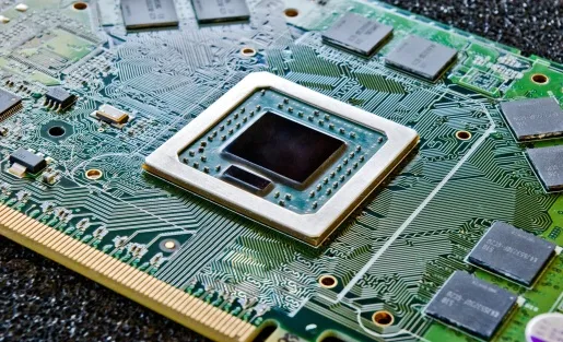
PCB plating refers to the process of depositing a thin layer of metal, often copper, nickel, or gold, onto the board’s surface or through-hole vias to improve conductivity and protect against corrosion. Plating is often a foundational step before applying a final surface finish. For instance, through-hole plating ensures reliable connections between layers in multilayer PCBs by coating the inside of drilled holes with copper, typically achieving a thickness of 0.8 to 1.2 mils (20-30 micrometers).
Plating is critical for maintaining signal integrity in high-frequency designs, where consistent conductivity is essential. However, plating alone isn’t always enough as a final surface finish because exposed copper can still oxidize. This is why additional finishes are applied over the plated layers to provide extra protection and solderability.
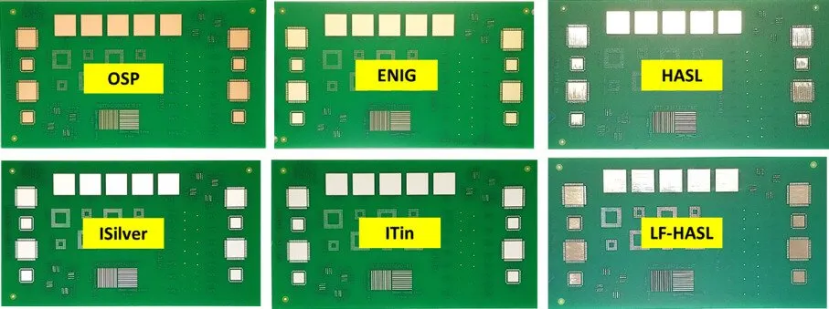
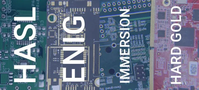
Common PCB Surface Finishes: ENIG, HASL, and OSP
While plating sets the stage, the final surface finish determines how well your PCB will perform in assembly and real-world conditions. Here, we’ll compare three popular surface finishes—ENIG, HASL, and OSP—focusing on their characteristics, advantages, and limitations.
1. ENIG (Electroless Nickel Immersion Gold)
ENIG is a two-layer finish consisting of a nickel barrier (typically 120-240 microinches thick) and a thin gold layer (2-8 microinches thick) on top. The nickel protects the copper from corrosion, while the gold ensures excellent solderability and prevents oxidation of the nickel layer.
Advantages:
- Superior corrosion resistance, ideal for harsh environments.
- Excellent solderability, even after long storage periods (shelf life of up to 12 months).
- Flat surface, perfect for fine-pitch components and surface-mount technology (SMT).
- Suitable for high-reliability applications like aerospace and medical devices.
Disadvantages:
- Higher cost compared to other finishes, often 2-3 times more expensive than HASL.
- Potential for "black pad" issues if the nickel layer is not properly applied, leading to weak solder joints.
- Not ideal for rework or multiple soldering cycles due to gold layer degradation.
Best For: High-end projects requiring long-term reliability and precise component placement.
2. HASL (Hot Air Solder Leveling)
HASL involves dipping the PCB into molten solder (traditionally tin-lead, now often lead-free due to environmental regulations) and using hot air to remove excess solder, leaving a thin, even coating (typically 40-400 microinches thick). It’s one of the oldest and most widely used surface finishes.
Advantages:
- Cost-effective, often the cheapest option for low-budget projects.
- Good solderability, as the surface is pre-coated with solder.
- Durable and suitable for through-hole components and hand soldering.
- Long shelf life (up to 12 months) if stored properly.
Disadvantages:
- Uneven surface, which can cause issues with fine-pitch or SMT components.
- Thermal shock during application can stress the board, potentially leading to warpage.
- Lead-free HASL may require higher soldering temperatures (up to 260°C), risking damage to sensitive components.
Best For: Simple, cost-sensitive projects with larger components and through-hole designs.
3. OSP (Organic Solderability Preservative)
OSP is a water-based, organic coating (0.2-0.5 micrometers thick) applied to the copper surface to prevent oxidation. It acts as a temporary barrier that preserves solderability until assembly.
Advantages:
- Environmentally friendly, as it contains no heavy metals or hazardous substances.
- Very low cost, often comparable to or cheaper than HASL.
- Flat surface, suitable for fine-pitch and SMT components.
- Simple application process, reducing manufacturing complexity.
Disadvantages:
- Short shelf life (typically 3-6 months), as the organic coating degrades over time.
- Poor corrosion resistance after soldering, not ideal for harsh environments.
- Not suitable for multiple reflow cycles or rework, as the coating burns off during soldering.
- Difficult to inspect visually for quality assurance due to its transparent nature.
Best For: Low-cost, short-turnaround projects with immediate assembly and minimal environmental exposure.
PCB Plating vs. Surface Finishes: Key Differences
While PCB plating and surface finishes are related, they serve different purposes. Plating is primarily about building conductive pathways and protecting internal structures like vias, often using copper or nickel as a base layer. Surface finishes, on the other hand, are the final protective and solderable coatings applied to the board’s exposed areas.
Here’s a quick comparison of how plating interacts with finishes like ENIG, HASL, and OSP:
- Plating: Focuses on conductivity and structural integrity, often a prerequisite for finishes. For example, ENIG builds on a plated nickel layer.
- ENIG: Adds corrosion resistance and solderability over plated layers, ideal for high-performance needs.
- HASL: Replaces or supplements plating with a solder layer, prioritizing cost over precision.
- OSP: Works directly on bare copper plating without additional metal layers, focusing on eco-friendliness and simplicity.
Understanding this relationship helps clarify why some projects might require robust plating followed by a specific finish, while others can skip complex plating steps with a simpler finish.
Comparison Table: ENIG vs. HASL vs. OSP
To make your decision easier, here’s a detailed comparison of the three surface finishes based on key criteria:
| Criteria | ENIG | HASL | OSP |
|---|---|---|---|
| Cost | High (2-3x HASL) | Low | Low |
| Solderability | Excellent | Good | Good (short-term) |
| Corrosion Resistance | Excellent | Good | Poor (post-soldering) |
| Shelf Life | 12 months | 12 months | 3-6 months |
| Surface Flatness | Excellent | Poor | Excellent |
| Best Application | High-reliability, fine-pitch | Cost-sensitive, through-hole | Short-turnaround, eco-friendly |
How to Choose the Right Surface Finish for Your Project
Selecting the best PCB surface finish involves balancing several factors based on your project’s requirements. Here are the key considerations to guide your choice:
1. Budget Constraints
If cost is a primary concern, HASL or OSP are the most economical options. ENIG, while more expensive, may save money in the long run for high-reliability projects by reducing failures and rework costs.
2. Component Type and Assembly Process
For boards with fine-pitch or SMT components, a flat surface is crucial—ENIG or OSP are better choices. HASL’s uneven surface can lead to misalignment or poor connections with smaller components.
3. Environmental Conditions
If your PCB will be exposed to humidity, temperature extremes, or corrosive environments, ENIG’s superior corrosion resistance makes it the top pick. OSP, on the other hand, struggles in harsh conditions after soldering.
4. Shelf Life and Storage
For projects with long storage times before assembly, ENIG or HASL are preferable due to their extended shelf life. OSP’s short shelf life makes it better for quick-turn projects.
5. Regulatory and Environmental Concerns
If your project must comply with strict environmental regulations, OSP’s eco-friendly nature is a significant advantage. Lead-free HASL is also an option, though it requires higher soldering temperatures.
Real-World Applications: Matching Finishes to Projects
To illustrate how these considerations play out, let’s look at a few hypothetical scenarios:
- Consumer Gadget Prototype: A low-cost gadget with a tight production timeline might use OSP for its affordability and quick assembly compatibility. The short shelf life isn’t an issue if assembly happens immediately.
- Industrial Control System: For a system exposed to varying temperatures and humidity, ENIG ensures long-term reliability despite its higher cost, protecting against corrosion and maintaining solderability.
- Hobbyist DIY Project: A simple circuit board with through-hole components can use HASL to keep costs down while providing a durable, solder-friendly surface for hand assembly.
Conclusion: Making an Informed Decision
Choosing between PCB plating and surface finishes like ENIG, HASL, and OSP is a pivotal step in ensuring the success of your electronics project. Each option offers distinct advantages—ENIG for reliability and precision, HASL for affordability and durability, and OSP for eco-friendliness and cost savings. By evaluating your project’s budget, component needs, environmental exposure, and timeline, you can select the finish that best aligns with your goals.
At ALLPCB, we’re committed to helping you navigate these choices with expert guidance and high-quality manufacturing solutions. Whether you’re tackling a complex industrial design or a simple prototype, understanding the nuances of PCB plating and surface finishes empowers you to build better, more reliable products. Take the time to assess your specific requirements, and you’ll be well on your way to a successful PCB design.


