 ALLPCB


In the fast-evolving world of autonomous vehicles, ensuring reliable communication between components is critical. One of the biggest hurdles in designing printed circuit boards (PCBs) for autonomous vehicle control systems is maintaining signal integrity. Signal integrity refers to the quality of an electrical signal as it travels through a PCB, ensuring it remains clear and undistorted. In high-speed systems like those in autonomous vehicles, poor signal integrity can lead to data errors, system failures, or even safety risks. This blog dives deep into the specific signal integrity challenges in autonomous vehicle control PCB design, focusing on high-speed PCB design, signal integrity simulation, controlled impedance PCB, automotive Ethernet PCB layout, and differential signaling PCB design. We'll explore practical solutions and actionable insights to help engineers tackle these challenges.
Why Signal Integrity Matters in Autonomous Vehicle PCBs
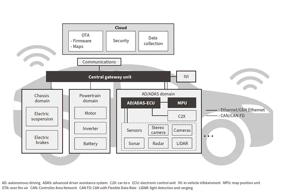
Autonomous vehicles rely on complex control systems to process data from sensors, cameras, and communication networks in real time. These systems demand high-speed data transmission, often exceeding several gigabits per second (Gbps). A single glitch or delay in signal transmission can disrupt critical functions like obstacle detection or braking. Signal integrity ensures that data signals remain accurate and timely as they travel across the PCB, avoiding issues like noise, crosstalk, or signal loss. In this high-stakes environment, even minor signal distortions can have catastrophic consequences, making signal integrity a top priority for PCB designers.
Key Signal Integrity Challenges in Autonomous Vehicle PCB Design
Designing PCBs for autonomous vehicle control systems presents unique challenges due to the high-speed, high-density, and safety-critical nature of these applications. Below, we break down the major signal integrity issues and how they impact performance.
1. High-Speed PCB Design: Managing Fast Data Rates
Autonomous vehicles process massive amounts of data from LiDAR, radar, and cameras, requiring high-speed PCB design to support data rates often above 10 Gbps. At such speeds, signal degradation becomes a significant concern. Issues like signal reflections, caused by impedance mismatches, and signal attenuation, due to long trace lengths, can distort data. For instance, a signal traveling at 10 Gbps on a PCB trace longer than 5 inches may experience noticeable loss if not designed with proper materials and layout techniques.
To address this, designers must use low-loss dielectric materials with a dielectric constant (Dk) below 3.5 to minimize signal attenuation. Additionally, keeping trace lengths as short as possible and avoiding sharp bends in routing can reduce reflections. High-speed PCB design also requires precise layer stack-up planning to ensure consistent signal paths and minimal interference.
2. Signal Integrity Simulation: Predicting and Preventing Issues
Before manufacturing a PCB, signal integrity simulation is essential to identify potential problems in the design. In autonomous vehicle systems, where reliability is non-negotiable, simulation tools help predict issues like crosstalk, jitter, and signal reflections. For example, a simulation might reveal that two adjacent traces carrying 5 Gbps signals are too close, causing crosstalk levels above 5% of the signal amplitude, which can corrupt data.
Using advanced simulation software, engineers can model the behavior of high-speed signals under various conditions, such as temperature changes or manufacturing tolerances. These simulations allow for adjustments in trace spacing, termination resistors, or via placement before the PCB is built, saving time and cost. Incorporating signal integrity simulation early in the design process is a proactive step to ensure robust performance in autonomous vehicle control systems.
3. Controlled Impedance PCB: Ensuring Signal Consistency
Controlled impedance PCB design is crucial for maintaining signal integrity in high-speed applications. Impedance mismatches between traces, connectors, and components can cause signal reflections, leading to data errors. In autonomous vehicle PCBs, where signals often operate at frequencies above 1 GHz, maintaining a target impedance (commonly 50 ohms for single-ended signals or 100 ohms for differential pairs) is vital.
Achieving controlled impedance involves precise calculations of trace width, spacing, and dielectric thickness. For instance, a trace width of 5 mils on a standard FR-4 material with a 4.5 Dk might be adjusted to 4 mils if a lower Dk material is used to maintain the same impedance. Designers must also account for manufacturing variations, as even a 10% deviation in trace width can alter impedance enough to degrade signal quality. Collaborating with a PCB fabrication partner to ensure tight tolerances is key to success in controlled impedance PCB design.
4. Automotive Ethernet PCB Layout: Supporting High-Speed Communication
Automotive Ethernet is becoming the backbone of in-vehicle networking for autonomous systems, offering data rates up to 10 Gbps for communication between control units. However, designing an automotive Ethernet PCB layout comes with unique signal integrity challenges. The high-speed nature of Ethernet signals makes them prone to electromagnetic interference (EMI) and crosstalk, especially in the noisy environment of a vehicle.
To mitigate these issues, designers should route Ethernet traces as differential pairs with tight coupling to minimize noise pickup. Keeping trace lengths matched within 5 mils ensures that signals arrive at the receiver simultaneously, avoiding timing errors. Additionally, placing ground planes beneath Ethernet traces and using shielding techniques can reduce EMI. A well-planned automotive Ethernet PCB layout is essential for reliable data transfer in autonomous vehicle systems.
5. Differential Signaling PCB Design: Reducing Noise in High-Speed Systems
Differential signaling PCB design is widely used in autonomous vehicle control systems to transmit high-speed data with minimal noise. Unlike single-ended signaling, differential signaling uses two complementary traces to carry a signal, canceling out common-mode noise and improving signal integrity. This is particularly important in autonomous vehicles, where electrical noise from motors, power systems, and external sources is common.
For effective differential signaling PCB design, traces must be routed with equal lengths and consistent spacing to maintain signal balance. A mismatch of even 10 mils in length can introduce skew, causing timing errors at data rates above 5 Gbps. Designers should also avoid routing differential pairs near noisy components or over split ground planes, as this can disrupt the signal path. By prioritizing symmetry and isolation in differential signaling PCB design, engineers can ensure cleaner, more reliable data transmission.
Environmental and Safety Challenges Impacting Signal Integrity
Beyond the technical aspects of PCB design, autonomous vehicle systems face environmental and safety challenges that further complicate signal integrity. These systems operate in harsh conditions, including temperature extremes from -40°C to 85°C, vibrations, and humidity. Such conditions can affect material properties, like the dielectric constant of PCB substrates, leading to impedance shifts and signal degradation.
Moreover, safety standards like ISO 26262 for automotive functional safety impose strict requirements on system reliability. A signal integrity failure in a PCB could violate these standards, risking certification issues or, worse, endangering lives. Designers must select materials and components rated for automotive environments and perform rigorous testing to validate signal integrity under worst-case scenarios.
Practical Solutions for Signal Integrity in Autonomous Vehicle PCBs
Overcoming signal integrity challenges in autonomous vehicle control PCB design requires a combination of best practices and advanced tools. Here are actionable strategies to ensure reliable performance:
- Material Selection: Choose low-loss materials with stable dielectric properties to minimize signal attenuation at high frequencies. Materials with a dissipation factor (Df) below 0.005 are ideal for high-speed designs.
- Trace Routing: Keep high-speed traces short and straight, avoiding 90-degree bends. Use 45-degree angles or curved traces to reduce reflections.
- Ground Planes: Implement solid, unbroken ground planes under high-speed signals to provide a consistent return path and reduce EMI.
- Termination Techniques: Use proper termination resistors (e.g., 50 ohms for single-ended signals) to match impedance and prevent reflections.
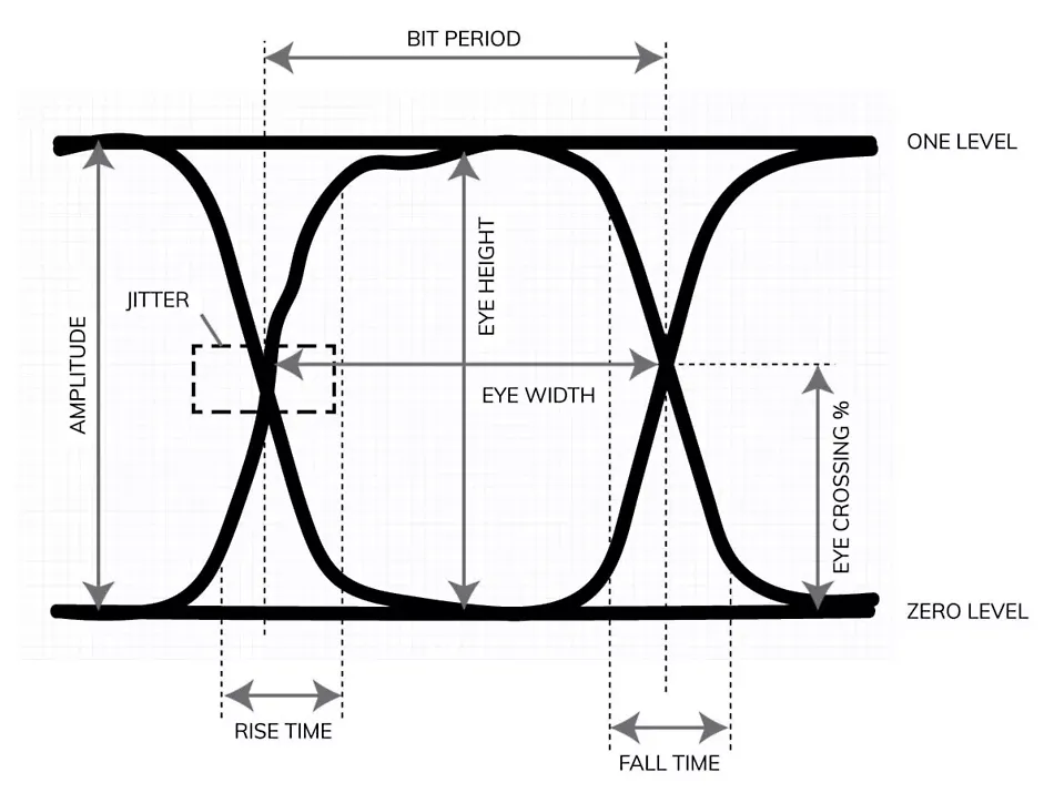
- Testing and Validation: Conduct thorough signal integrity testing, such as eye diagram analysis, to measure jitter and signal quality. An eye diagram opening of at least 80% at 10 Gbps indicates good signal integrity.
Future Trends in Autonomous Vehicle PCB Design
As autonomous vehicle technology advances, PCB design must keep pace with increasing data rates and complexity. Emerging standards like 25 Gbps automotive Ethernet and PCIe 5.0 will push signal integrity requirements even further. Additionally, the integration of artificial intelligence (AI) for real-time decision-making will demand even denser PCB layouts, increasing the risk of crosstalk and interference.
To stay ahead, designers will need to adopt advanced simulation tools, explore innovative materials, and embrace automation in PCB layout processes. Staying informed about industry trends and collaborating with experienced fabrication partners can help navigate these future challenges.
Conclusion
Signal integrity is a cornerstone of reliable autonomous vehicle control PCB design. With the high-speed, high-stakes nature of these systems, addressing challenges like signal degradation, crosstalk, and EMI is essential for safety and performance. By focusing on high-speed PCB design, leveraging signal integrity simulation, implementing controlled impedance PCB techniques, optimizing automotive Ethernet PCB layout, and mastering differential signaling PCB design, engineers can build robust systems that meet the demands of autonomous driving. At ALLPCB, we are committed to supporting designers with the tools, resources, and expertise needed to tackle these challenges and bring innovative solutions to life.


