 ALLPCB


If you're looking to understand the internal quality of a printed circuit board (PCB), microsectioning, also known as cross-section analysis, is a vital process. This technique allows engineers and manufacturers to inspect the hidden layers, plating, and connections within a PCB to ensure it meets quality standards. In this comprehensive guide, we'll dive deep into PCB microsectioning sample preparation, explore microsectioning equipment for PCBs, and explain the metallographic preparation of PCBs. Whether you're a seasoned engineer or new to PCB analysis, this article will equip you with the knowledge to master cross-section analysis.
What Is PCB Microsectioning and Why Does It Matter?
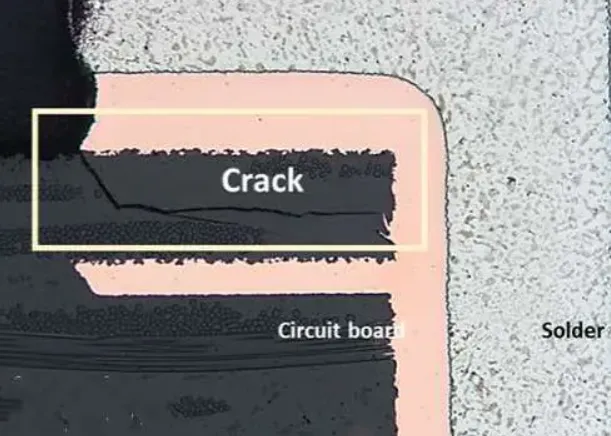
PCB microsectioning is a destructive testing method where a small section of a circuit board is cut, mounted, and polished to reveal its internal structure. This process, often referred to as cross-sectioning or metallographic preparation, helps evaluate the quality of plated-through holes (PTHs), vias, copper plating thickness, and solder joints. By examining these elements under a microscope, manufacturers can identify defects like voids, cracks, or insufficient plating that could lead to board failure.
Why is this important? In industries like aerospace, automotive, and consumer electronics, even a tiny flaw in a PCB can cause significant issues, from signal loss to complete system failure. Microsectioning ensures that boards meet strict standards, such as those set by the Institute of Printed Circuits (IPC), before they are used in critical applications.
Key Benefits of PCB Microsectioning
- Quality Assurance: Detects internal defects that are invisible to the naked eye.
- Failure Analysis: Helps pinpoint the root cause of PCB failures during testing or after deployment.
- Process Validation: Confirms that manufacturing processes, like plating or drilling, are within specifications.
- Compliance: Ensures adherence to industry standards for reliability and performance.
Understanding PCB Microsectioning Sample Preparation
Preparing a PCB sample for microsectioning is a meticulous process that requires precision to avoid damaging the internal structures you want to analyze. Proper preparation ensures that the cross-section is clear and ready for microscopic inspection. Let's break down the key steps involved in PCB microsectioning sample preparation.
Step 1: Cutting the Sample
The first step is to cut a small, representative section from the PCB. This is typically done using a precision saw with a diamond blade to minimize damage to the delicate layers. The sample size is usually small, often around 1-2 inches in length, to make it manageable for mounting and polishing.
Step 2: Mounting the Sample
Once cut, the sample is embedded in a mounting material, such as epoxy resin, to provide support during grinding and polishing. The mounting material must fully encase the sample to prevent movement or distortion. This step is crucial for maintaining the integrity of the PCB’s internal features, like vias or solder joints.
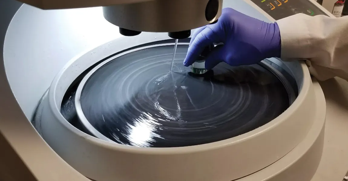
Step 3: Grinding and Polishing
After mounting, the sample undergoes grinding to remove excess material and expose the desired cross-section. This is followed by polishing with progressively finer abrasives to achieve a smooth, mirror-like finish. A well-polished surface is essential for clear microscopic analysis, as scratches or unevenness can obscure critical details.
Step 4: Etching (Optional)
In some cases, the polished sample is etched with a chemical solution to enhance the visibility of certain features, such as grain boundaries in copper plating. Etching can highlight defects or inconsistencies that might not be visible otherwise.
T? Assistant: Tips for Successful PCB Microsectioning Sample Preparation
- Use Proper Equipment: Invest in a high-quality precision saw and polishing machine to avoid damaging the sample.
- Work Slowly: Rushing the grinding or polishing process can introduce artifacts or scratches that distort the analysis.
- Control Temperature: Excessive heat during cutting or grinding can melt or deform the PCB materials, so use coolant if necessary.
- Document Everything: Record the location of the sample on the PCB, the preparation steps, and any observations to ensure traceability.
Microsectioning Equipment for PCBs: Tools You Need
To achieve accurate and reliable results, having the right microsectioning equipment for PCBs is essential. The tools used in this process are specialized to handle the delicate nature of circuit boards and ensure precision at every stage. Below, we’ll explore the key equipment needed for effective PCB cross-section analysis.
1. Precision Cutting Saw
A precision cutting saw with a thin diamond blade is used to extract a small section from the PCB without causing mechanical stress or delamination. These saws often feature adjustable speeds and cooling systems to prevent overheating. Cutting accuracy is critical, as a poorly cut sample can lead to misleading analysis results.
2. Mounting Press
A mounting press or vacuum impregnation system is used to encase the PCB sample in epoxy or resin. This equipment ensures that the sample is securely held in place during grinding and polishing, preventing movement that could damage the cross-section.
3. Grinding and Polishing Machine
Grinding and polishing machines are designed to systematically remove material from the sample and create a smooth surface for analysis. These machines often have rotating platens and use abrasive discs or slurries with varying grit sizes (e.g., starting at 120 grit and finishing at 4000 grit) to achieve a high-quality finish.
4. Optical Microscope
Once the sample is prepared, an optical microscope with magnification capabilities of 50x to 1000x is used to inspect the cross-section. Some advanced setups include digital imaging systems to capture and analyze images for documentation and reporting.
5. Etching Solutions and Accessories
For enhanced visibility of certain features, chemical etching solutions may be applied. Proper storage containers, safety gear, and application tools are necessary to handle these chemicals safely.
Choosing the Right Equipment
When selecting microsectioning equipment for PCBs, consider factors like the volume of samples you’ll be processing and the level of precision required. High-volume labs may benefit from automated systems, while smaller operations can start with manual tools. Ensure that the equipment meets industry standards for materialographic preparation to guarantee accurate results.
Metallographic Preparation of PCBs: A Deeper Dive
Metallographic preparation of PCBs is a broader term that encompasses the entire process of preparing a sample for microscopic analysis, including cutting, mounting, grinding, polishing, and etching. This preparation is critical for revealing the microstructure of the PCB materials, such as copper layers, dielectric materials, and solder joints.
Why Metallographic Preparation Matters
The goal of metallographic preparation is to create a sample that accurately represents the PCB’s internal structure without introducing artifacts or damage. For example, improper grinding can cause smearing of copper layers, making it appear thicker than it actually is. Such errors can lead to incorrect conclusions about the board’s quality or performance.
Key Measurements in Metallographic Analysis
During analysis, several critical parameters are measured to assess the PCB’s quality:
- Copper Plating Thickness: Typically measured in microns, plating thickness in PTHs should meet IPC standards (e.g., a minimum of 25 microns for Class 3 boards).
- Via Integrity: Checking for voids or cracks in vias that could disrupt electrical conductivity.
- Layer Alignment: Ensuring that internal layers are properly aligned with a tolerance often as tight as ±50 microns.
- Solder Joint Quality: Evaluating the wetting and bonding of solder to confirm reliability under thermal or mechanical stress.
Common Challenges in Metallographic Preparation
Metallographic preparation of PCBs comes with several challenges that can affect the accuracy of the analysis:
- Material Variability: PCBs are made of composite materials like FR-4, which have different hardness levels, making uniform grinding difficult.
- Heat Sensitivity: Excessive heat during cutting or grinding can alter the sample’s properties, such as melting solder or epoxy.
- Edge Retention: Ensuring that the edges of the sample remain intact during preparation to avoid losing critical data.
How Microsectioning Supports PCB Quality Control
Microsectioning is a cornerstone of PCB quality control, providing insights that non-destructive testing methods like X-ray inspection cannot. By physically exposing the internal structure, engineers can verify that manufacturing processes are consistent and that the board will perform as expected under real-world conditions.
Applications in Manufacturing
- Process Optimization: Identifying variations in plating or drilling processes to improve consistency.
- Prototype Validation: Confirming that prototype designs meet specifications before mass production.
- Failure Investigation: Analyzing returned or failed boards to determine if the issue lies in design, materials, or assembly.
Industry Standards and Compliance
Microsectioning is often performed to comply with standards like IPC-A-600, which defines acceptability criteria for PCBs. For instance, the standard specifies that copper plating in vias must have no more than a 20% reduction in thickness at any point to ensure reliability. Adhering to such guidelines through microsectioning helps manufacturers deliver high-quality products and avoid costly recalls.
Best Practices for Effective PCB Microsectioning
To ensure the best results from PCB microsectioning, follow these best practices:
- Standardize Procedures: Develop a consistent workflow for sample preparation and analysis to minimize variability.
- Calibrate Equipment: Regularly calibrate cutting, grinding, and measurement tools to maintain accuracy.
- Train Personnel: Ensure that staff are well-trained in handling delicate samples and operating specialized equipment.
- Use High-Quality Consumables: Opt for premium abrasives, resins, and etching chemicals to achieve clear, reliable cross-sections.
Conclusion: Mastering PCB Cross-Section Analysis
PCB microsectioning is an indispensable tool for ensuring the quality and reliability of printed circuit boards. From PCB microsectioning sample preparation to selecting the right microsectioning equipment for PCBs and mastering metallographic preparation of PCBs, every step plays a critical role in uncovering the hidden details of a board’s internal structure. By following the guidelines and best practices outlined in this guide, you can enhance your ability to detect defects, validate processes, and deliver high-performing PCBs for any application.
Whether you’re analyzing a single prototype or managing high-volume production, investing time and resources into effective cross-section analysis will pay off in improved product quality and customer satisfaction. With the right tools and techniques, you’ll be well-equipped to tackle the challenges of PCB manufacturing and stay ahead in a competitive industry.


