 ALLPCB


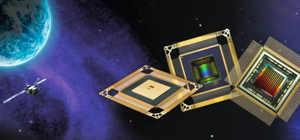
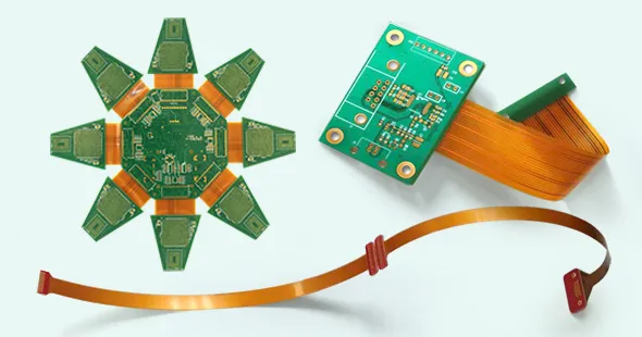
In the realm of space exploration, where every component must withstand extreme conditions and perform flawlessly, flexible PCBs (Printed Circuit Boards) have emerged as a critical technology. These lightweight, adaptable circuits are ideal for the compact and dynamic needs of spacecraft and satellites. However, designing a flexible PCB for space comes with unique hurdles, from material selection to ensuring reliability under harsh conditions. In this comprehensive guide, we’ll dive into the design challenges of using flexible PCBs in space applications and explore solutions to overcome them, focusing on key aspects like materials, bend radius, adhesives, and dynamic bending.
Why Flexible PCBs Are Essential for Space Applications
Flexible PCBs offer distinct advantages over traditional rigid boards in space missions. Their ability to bend and conform to tight spaces makes them perfect for satellites, rovers, and other spacecraft where weight and volume are critical. They reduce the need for connectors and cables, minimizing points of failure while saving on mass—a crucial factor when launch costs can exceed $10,000 per kilogram. Additionally, their adaptability supports dynamic movements, such as solar panel adjustments or robotic arm operations, which are common in space environments.
Despite these benefits, the harsh conditions of space—extreme temperatures ranging from -150°C to 150°C, vacuum environments, and intense radiation—pose significant challenges. Designing a flex PCB that can endure these factors while maintaining performance requires careful planning and innovative solutions.
Design Challenges for Flexible PCBs in Space
Creating a reliable flexible PCB for space applications involves addressing several complex challenges. Below, we break down the key obstacles and discuss strategies to overcome them.
1. Material Selection: Choosing Flex PCB Materials for Extreme Environments
The materials used in a flexible PCB must withstand the brutal conditions of space. Standard materials often fail under thermal cycling, radiation exposure, and outgassing in a vacuum. For instance, temperature swings can cause expansion and contraction, leading to cracks or delamination if the material isn’t suited for such stress.
Polyimide is a popular choice for flex PCB materials for extreme environments due to its excellent thermal stability, withstanding temperatures from -269°C to 400°C, and resistance to radiation. It also has low outgassing properties, which prevents contamination in vacuum conditions. For added durability, copper cladding in flex PCBs is often designed with rolled annealed (RA) copper, which offers better flexibility and fatigue resistance compared to electrodeposited copper, especially during repeated bending cycles.
Another consideration is dielectric strength, which ensures insulation under high-voltage conditions often encountered in space electronics. A typical polyimide layer might have a dielectric strength of 3,000 volts per mil, providing robust protection against electrical breakdown. However, engineers must balance material performance with cost, as high-grade materials can significantly increase production expenses.
To mitigate risks, thorough testing under simulated space conditions is essential. This includes thermal-vacuum testing to replicate the environment and radiation testing to ensure materials won’t degrade over time.
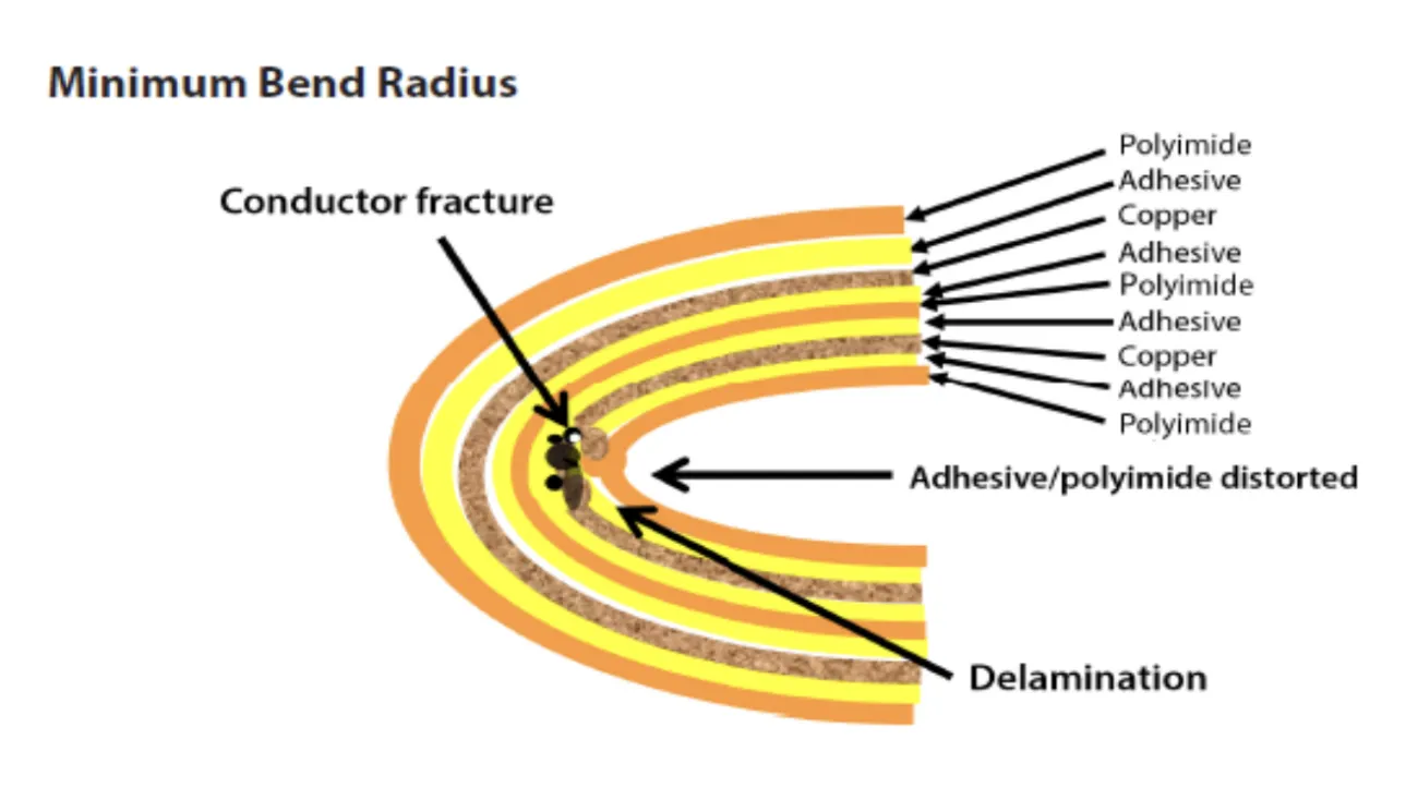
2. Defining the Right Bend Radius for Space-Grade Flex PCBs
The bend radius—the minimum radius a flex PCB can be bent without damage—is a critical factor in design. In space applications, where components often need to fold or flex repeatedly, an improper bend radius for space-grade flex PCBs can lead to cracking of copper traces or material fatigue, resulting in circuit failure.
For a single-layer flex PCB, the minimum bend radius is typically calculated as 6 times the thickness of the board. For multilayer designs, this increases to 12 times the thickness or more, depending on the stack-up. For example, a 0.2 mm thick single-layer flex PCB should have a minimum bend radius of 1.2 mm to avoid stress on the copper traces. Exceeding this limit can reduce the lifespan of the PCB, especially in dynamic applications like deployable antennas or robotic mechanisms.
Designers must also consider the placement of components and traces near bend areas. Keeping critical traces perpendicular to the bend line and avoiding vias in high-stress zones can prevent failures. Using teardrop-shaped pads for vias, rather than circular ones, can further reduce stress concentration by distributing forces more evenly.
Simulation tools are invaluable for predicting how a flex PCB will behave under bending stress. Finite Element Analysis (FEA) can model the mechanical strain on the board, helping engineers optimize the bend radius for space-grade flex PCBs before manufacturing.
3. Adhesive Selection for Flex PCBs in Space: Ensuring Reliability
Adhesives play a vital role in bonding layers of a flexible PCB, but selecting the right adhesive for space applications is challenging. The wrong choice can lead to delamination, outgassing, or loss of bond strength under extreme conditions. Adhesive selection for flex PCBs in space must prioritize thermal stability, low outgassing, and compatibility with the vacuum of space.
Acrylic adhesives are often avoided in space applications due to their higher outgassing rates, which can contaminate sensitive equipment. Instead, adhesive-less constructions using direct bonding of polyimide and copper are preferred for their stability and minimal outgassing. When adhesives are necessary, epoxy-based options with low Total Mass Loss (TML) and Collected Volatile Condensable Materials (CVCM) values are ideal. NASA standards, such as those outlined in SP-R-0022A, recommend materials with TML less than 1.0% and CVCM less than 0.1% to ensure safety in vacuum environments.
Thermal cycling also affects adhesive performance. An adhesive must maintain its bond strength through hundreds or thousands of temperature cycles without cracking or degrading. Testing under simulated space conditions can help validate adhesive choices, ensuring they meet mission requirements.
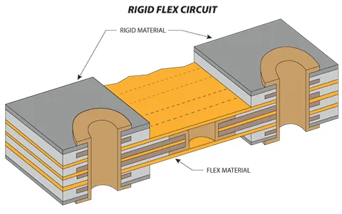
4. Addressing Dynamic Bending Applications in Space
Spacecraft often involve moving parts, such as solar arrays, antennas, or robotic limbs, where flex PCBs must endure repeated bending. Dynamic bending applications in space require designs that can handle thousands of flex cycles without failure, all while exposed to extreme environmental stressors.
The fatigue life of a flex PCB in dynamic bending is influenced by the bend radius, material properties, and trace design. For instance, using thinner copper layers (e.g., 0.5 oz/ft2 instead of 1 oz/ft2) can improve flexibility and reduce stress during bending, extending the board’s lifespan. However, thinner copper may increase resistance, so designers must balance flexibility with electrical performance. A typical signal trace in a space-grade flex PCB might be designed for an impedance of 50 ohms to ensure reliable signal transmission, requiring precise control over trace width and dielectric thickness.
Stiffeners can be added to areas of the PCB that don’t require bending, providing mechanical support for component mounting while allowing flexibility in dynamic regions. Additionally, strain relief features, such as curved traces or mesh patterns in high-flex areas, can minimize stress on the copper during movement.
Reliability testing for dynamic bending often involves flex cycle testing, where the PCB is bent repeatedly under controlled conditions. For space applications, this testing should also simulate thermal and vacuum environments to ensure performance under real-world conditions. A flex PCB designed for a solar array might need to withstand 10,000 bend cycles over a 10-year mission lifespan, making durability a top priority.
Best Practices for Designing Flexible PCBs for Space
To ensure success, engineers should follow these best practices when designing a flexible PCB for space applications:
- Collaborate Early with Manufacturers: Work closely with your PCB fabrication partner to select materials and processes that meet space-grade standards. Early collaboration can prevent costly redesigns.
- Prioritize Testing: Conduct extensive environmental testing, including thermal cycling, radiation exposure, and dynamic flexing, to validate designs before deployment.
- Optimize Stack-Up Design: Keep the layer count as low as possible to reduce thickness and improve flexibility, while ensuring electrical performance with controlled impedance traces.
- Document Requirements: Clearly define mission-specific requirements, such as temperature ranges, radiation tolerance, and flex cycles, to guide material and design choices.
Future Trends in Flexible PCB Technology for Space
As space exploration advances, so does the technology behind flexible PCBs. Emerging trends include the use of advanced composites for even greater thermal and radiation resistance, as well as the integration of embedded sensors within flex PCBs to monitor structural health in real-time. Additionally, additive manufacturing techniques are being explored to create ultra-thin, highly customizable flex circuits that can further reduce weight and improve performance.
These innovations promise to make flexible PCBs even more integral to future missions, from lunar bases to deep-space probes, where reliability and adaptability are paramount.
Conclusion
Flexible PCBs are transforming the way we design electronics for space applications, offering unmatched versatility and compactness. However, overcoming the design challenges associated with a flexible PCB for space requires meticulous attention to material selection, bend radius, adhesive choices, and dynamic bending performance. By leveraging high-performance flex PCB materials for extreme environments, optimizing the bend radius for space-grade flex PCBs, making informed decisions on adhesive selection for flex PCBs in space, and designing for dynamic bending applications in space, engineers can create reliable solutions for the harshest conditions imaginable.


