 ALLPCB


Designing and manufacturing flex PCBs, especially their inner layers, can be a complex task. If you're searching for insights on flexible PCB inner layer routing, flex PCB material selection for inner layers, or rigid-flex PCB inner layer challenges, you're in the right place. This blog dives deep into the critical aspects of flex PCB inner layer design and manufacturing, addressing common hurdles and offering practical solutions for engineers and designers. From material choices to routing techniques, we'll cover everything you need to know to ensure your flex PCB performs reliably and meets industry standards.
What Are Flex PCB Inner Layers and Why Do They Matter?
Flex PCBs, or flexible printed circuit boards, are designed to bend and conform to unique shapes, making them ideal for compact and dynamic applications like wearables, medical devices, and aerospace systems. The inner layers of a flex PCB are the hidden conductive layers sandwiched between insulating materials. These layers carry critical signals and power, and their design directly impacts the board's performance, reliability, and manufacturability.
Inner layers in flex PCBs face unique challenges compared to rigid PCBs. They must withstand repeated bending without cracking, maintain signal integrity under stress, and be compatible with the flexible materials used. Poor design or material choices can lead to failures like delamination, trace breakage, or signal loss. Understanding these challenges is the first step to creating a robust flex PCB design.
Key Design Challenges for Flex PCB Inner Layers
Designing inner layers for flex PCBs requires careful planning to balance flexibility, durability, and electrical performance. Below are some of the most common challenges engineers face during the design phase.
1. Flexible PCB Inner Layer Routing: Precision Under Stress
Routing traces in the inner layers of a flex PCB is far more complex than in rigid boards. The traces must endure bending and twisting without breaking or losing conductivity. One major challenge is maintaining a minimum bend radius—typically recommended as 10 times the thickness of the PCB for dynamic flex applications. Tighter bends can cause stress concentrations, leading to micro-cracks in copper traces.
To mitigate this, designers often use curved traces instead of sharp 90-degree angles, as curves distribute stress more evenly. Additionally, staggering traces across layers prevents overlapping stress points, reducing the risk of failure. For high-speed signals, maintaining controlled impedance is critical. A typical flex PCB might target an impedance of 50 ohms for single-ended signals, requiring precise trace width and spacing calculations, often around 0.1 mm for inner layers, depending on the dielectric material.
Another routing challenge is via placement. Vias in flex areas can become weak points under bending stress. Using teardrop-shaped vias or larger annular rings (e.g., 0.3 mm or more) can improve reliability by reducing the risk of pad lifting or cracking.

2. Signal Integrity and Crosstalk in Inner Layers
Signal integrity is a significant concern in flex PCB inner layers, especially for high-speed applications. The flexible nature of the board can introduce variations in dielectric thickness, affecting impedance and causing signal reflections. For instance, a dielectric constant mismatch between layers can lead to signal delays or losses, with typical dielectric constants for polyimide materials ranging from 3.2 to 3.5.
Crosstalk between adjacent traces in inner layers is another issue, particularly in densely packed designs. To minimize crosstalk, designers should maintain adequate spacing—often at least 3 times the trace width—and consider using ground planes or shielding layers. These techniques help isolate signals and reduce electromagnetic interference (EMI), ensuring data rates of up to 10 Gbps or more remain stable in critical applications.
3. Thermal Management in Confined Spaces
Flex PCBs often operate in tight spaces where heat dissipation is limited. Inner layers can trap heat, leading to thermal stress that affects both the copper traces and the surrounding materials. Without proper thermal vias or heat-spreading techniques, temperatures can rise above safe limits, typically 85°C for standard flex materials, risking delamination or material degradation.
Designers can address this by incorporating thermal vias to transfer heat to outer layers or by using materials with higher thermal conductivity. Careful placement of heat-generating components away from bend areas also helps protect inner layers from thermal stress during operation.
Flex PCB Material Selection for Inner Layers: Getting It Right
Choosing the right materials for flex PCB inner layers is critical to achieving flexibility, durability, and performance. Material selection directly influences how well the inner layers handle bending, thermal stress, and electrical demands. Let’s explore the key considerations for flex PCB material selection for inner layers.
1. Base Materials: Polyimide as the Standard
Polyimide is the most common base material for flex PCBs due to its excellent flexibility, thermal stability, and chemical resistance. It can withstand temperatures up to 260°C, making it suitable for soldering and harsh environments. For inner layers, polyimide films with thicknesses of 12.5 to 50 microns are often used, balancing flexibility with structural integrity.
However, not all polyimide materials are created equal. Adhesive-less polyimide laminates are preferred for inner layers because they reduce the risk of delamination during bending. Traditional adhesive-based laminates can fail under repeated flexing, especially in dynamic applications, as the adhesive layer weakens over time.
2. Copper Foil Selection for Conductive Layers
The copper foil used in inner layers must also be chosen carefully. Rolled annealed (RA) copper is the standard for flex PCBs because it is more ductile than electrodeposited (ED) copper, allowing it to bend without cracking. Typical copper thicknesses for inner layers range from 9 to 35 microns, with thinner foils preferred for tighter bend radii.
A challenge with RA copper is its higher cost and limited availability in very thin forms. Designers must weigh the benefits of flexibility against budget constraints, ensuring the copper can handle the required current density—often 1-3 A/mm2 for most applications—without overheating.
3. Dielectric and Coverlay Materials
The dielectric material between inner layers must maintain consistent electrical properties under flexing. Polyimide dielectrics are again the go-to choice, with a typical thickness of 25 microns for multilayer flex designs. For high-frequency applications, low-loss materials with a dissipation factor below 0.005 are essential to minimize signal attenuation.
Coverlay, the protective layer over inner traces, also plays a role in material selection. It must be flexible yet durable, often made from polyimide with a thickness of 25-50 microns. Proper adhesion of the coverlay to inner layers prevents moisture ingress and mechanical damage during bending.
Rigid-Flex PCB Inner Layer Challenges: Bridging Two Worlds
Rigid-flex PCBs combine the benefits of rigid and flexible boards, but their inner layers present unique challenges. The transition zones between rigid and flex areas are particularly prone to stress, requiring careful design and manufacturing techniques for rigid-flex PCB inner layers.
1. Managing Transition Zones
The transition from rigid to flex areas is a common failure point in rigid-flex designs. Inner layers in the flex region must bend without affecting the rigid section, where components are mounted. A typical design rule is to avoid placing vias or high-density routing in transition zones, as these areas experience high mechanical stress. Gradual transitions with a bend radius of at least 1.5 mm help reduce strain on inner layers.
Another technique is to use bookbinder construction, where flex layers are bonded only at specific points to the rigid section, allowing independent movement. This approach minimizes stress on inner layer traces but requires precise alignment during manufacturing.
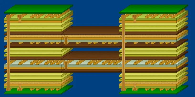
2. Layer Stack-Up Complexity
Rigid-flex PCBs often have complex stack-ups, with inner layers varying between rigid and flex materials. For example, a 6-layer rigid-flex design might have 4 rigid layers and 2 flex layers, with inner traces needing to maintain continuity across both. Misalignment during lamination can cause open circuits or shorts, especially if the flex inner layers shift by even 0.1 mm.
To address this, designers use registration marks and optical alignment systems during manufacturing. Specifying tighter tolerances, such as ±0.05 mm for layer-to-layer alignment, ensures inner layer traces connect properly across rigid and flex regions.

Manufacturing Challenges for Flex PCB Inner Layers
Even with a flawless design, manufacturing flex PCB inner layers comes with its own set of hurdles. These challenges often stem from the unique properties of flexible materials and the precision required for multilayer builds.
1. Lamination and Delamination Risks
Laminating multiple layers in a flex PCB requires precise control of temperature and pressure. Excessive heat (above 180°C for prolonged periods) or uneven pressure can cause inner layers to warp or delaminate. Delamination is particularly problematic in dynamic flex applications, where repeated bending exacerbates weak bonds between layers.
Manufacturers mitigate this by using low-flow or no-flow prepregs in rigid-flex designs and by conducting thorough testing, such as thermal cycling between -40°C and 125°C, to ensure layer adhesion. Designers can help by specifying adhesive-less materials for inner layers, as mentioned earlier.
2. Drilling and Via Formation
Drilling vias through flex PCB inner layers is trickier than in rigid boards due to the softer materials. Misaligned drills can tear polyimide or cause burrs in copper, leading to unreliable connections. Laser drilling is often used for microvias in flex designs, achieving diameters as small as 0.05 mm with high precision, though it increases production costs.
Plating vias in flex PCBs also poses challenges. Uneven plating thickness can weaken inner layer connections, especially under bending stress. Specifying a minimum plating thickness of 20 microns ensures durability, though it must be balanced with flexibility requirements.
3. Testing and Quality Control
Testing flex PCB inner layers for defects is more complex due to their hidden nature and flexible properties. Standard automated optical inspection (AOI) may miss inner layer issues like micro-cracks or impedance mismatches. Advanced techniques like X-ray inspection or time-domain reflectometry (TDR) are often needed to verify inner layer integrity, especially for high-speed designs targeting 50-ohm impedance.
Manufacturers also perform flex testing, simulating thousands of bend cycles (e.g., 10,000 cycles at a 10 mm radius) to ensure inner layers won’t fail in real-world use. Designers should collaborate closely with manufacturers to define testing protocols that match the application’s demands.
Best Practices for Flex PCB Inner Layer Design and Manufacturing
To overcome the challenges discussed, here are some actionable best practices for designing and manufacturing flex PCB inner layers:
- Optimize Routing: Use curved traces and avoid sharp angles in flexible PCB inner layer routing. Stagger traces across layers to distribute stress evenly.
- Choose Materials Wisely: Prioritize adhesive-less polyimide and RA copper for flex PCB material selection for inner layers, ensuring flexibility and durability.
- Focus on Transitions: In rigid-flex PCB inner layers, design gradual transitions and avoid high-stress features like vias in bend areas.
- Specify Tolerances: Work with manufacturers to define tight alignment and plating tolerances for inner layers, preventing shorts or open circuits.
- Test Thoroughly: Incorporate flex cycle testing and advanced inspection methods to validate inner layer performance before full production.
Conclusion: Mastering Flex PCB Inner Layers
Designing and manufacturing flex PCB inner layers is no small feat. From tackling flexible PCB inner layer routing challenges to making informed decisions about flex PCB material selection for inner layers, every step requires precision and foresight. For rigid-flex PCB inner layers, managing transitions and stack-up complexity adds another layer of difficulty. By understanding these challenges and following best practices, engineers can create reliable, high-performing flex PCBs that meet the demands of modern applications.
Whether you're working on a wearable device, a medical sensor, or an aerospace system, paying attention to inner layer design and manufacturing will ensure your flex PCB stands up to real-world conditions. With the right approach, you can turn these challenges into opportunities for innovation and success in your next project.


