 ALLPCB


If you're looking for ways to achieve PCB cost reduction while maintaining impedance control, you're in the right place. Designing impedance-controlled printed circuit boards (PCBs) doesn't have to break the bank. By focusing on smart layer count decisions, strategic material selection, and optimized stackup designs, you can significantly lower PCB manufacturing costs without sacrificing performance. In this guide, we'll dive deep into practical strategies for cheap impedance control that ensure signal integrity for high-speed applications while keeping your budget in check.
Whether you're an engineer working on high-frequency designs or a procurement specialist aiming to cut costs, this blog will walk you through actionable tips and detailed insights to help you balance performance and affordability in your PCB projects.
Why Impedance Control Matters in PCB Design
Before we explore cost-saving strategies, let's understand why impedance control is critical. In high-speed digital circuits, such as those used in telecommunications, computing, and RF applications, maintaining consistent impedance is essential for signal integrity. If the impedance of a trace doesn't match the source or load, it can lead to signal reflections, crosstalk, and data loss. For instance, a typical high-speed design might target a characteristic impedance of 50 ohms for single-ended traces or 100 ohms for differential pairs to ensure proper signal transmission.
However, achieving this precision often comes with higher PCB manufacturing costs due to tighter tolerances, specialized materials, and complex stackups. The good news is that with the right approach, you can implement cheap impedance control without compromising quality. Let's explore how to do that through cost-effective stackup strategies.

Strategy 1: Optimize Layer Count for Cost Reduction
One of the most impactful ways to reduce PCB manufacturing costs is by carefully choosing the layer count. Each additional layer increases fabrication complexity, material usage, and testing requirements, driving up costs. Here's how to approach this:
- Minimize Layers: For many high-speed designs, a 4-layer or 6-layer PCB can suffice instead of jumping to 8 or more layers. For example, a 4-layer board with two signal layers and two ground planes can often provide adequate impedance control for signals up to 5 GHz if designed properly.
- Use Ground Planes Effectively: Place ground planes adjacent to signal layers to create a stable reference for impedance. This reduces the need for additional layers solely for reference planes, cutting down on costs.
- Evaluate Design Needs: Assess whether your design truly requires multiple layers. If your circuit operates below 1 GHz, a simpler stackup with fewer layers might still meet impedance targets without extra expense.
By reducing the layer count, you can achieve significant PCB cost reduction while maintaining performance. However, always simulate your design to ensure that fewer layers don't compromise signal integrity.
Strategy 2: Smart Material Selection for Cheap Impedance Control
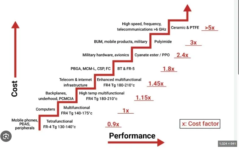
The choice of materials plays a huge role in both impedance control and PCB manufacturing costs. High-performance materials like Rogers or Isola are often used for strict impedance requirements due to their stable dielectric constants (Dk) and low loss tangents (Df). However, these materials can be expensive. Here's how to approach material selection for cost savings:
- Standard FR-4 for Lower Frequencies: For designs operating below 2 GHz, standard FR-4 materials with a Dk of around 4.2-4.6 can often meet impedance needs at a fraction of the cost of premium laminates. This is ideal for many consumer electronics and industrial applications.
- Hybrid Stackups: If high-frequency signals are limited to specific layers, consider a hybrid approach. Use cost-effective FR-4 for power and ground layers, and reserve higher-grade materials only for critical signal layers. This can reduce costs by up to 30% compared to full high-end material stackups.
- Work with Manufacturers: Collaborate with your PCB fabricator to identify alternative materials with similar electrical properties but lower costs. Many manufacturers offer in-house material options that balance performance and affordability.
By making informed decisions on material selection, you can achieve cheap impedance control without sacrificing the reliability of your high-speed signals.
Strategy 3: Design Stackups for Impedance and Cost Efficiency
The stackup design directly influences both impedance control and manufacturing complexity. A well-planned stackup can help you avoid costly over-design while meeting performance goals. Consider these tips:
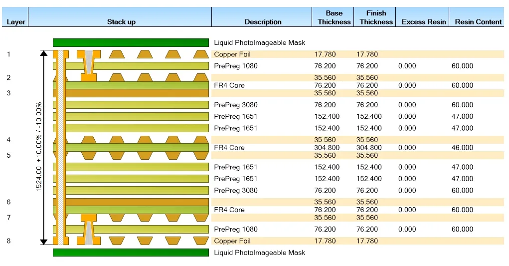
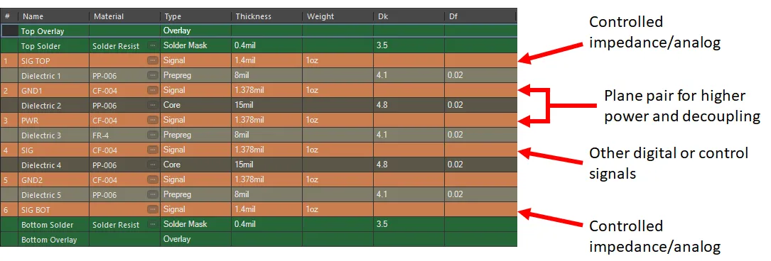
- Symmetrical Stackups: Design symmetrical stackups to prevent warping during fabrication, which can lead to impedance inconsistencies and costly rework. For instance, in a 6-layer board, ensure that dielectric thicknesses and copper weights are balanced on both sides of the core.
- Control Dielectric Thickness: Impedance is heavily influenced by the distance between signal traces and their reference planes. Use thinner dielectrics (e.g., 4-5 mils) for tighter impedance control, but avoid going below the manufacturer's minimum to prevent added costs. A common target for 50-ohm traces on FR-4 is a dielectric thickness of around 6 mils with a trace width of 5-7 mils.
- Wider Traces When Possible: Wider traces are easier and cheaper to fabricate with consistent impedance. Narrow traces require tighter tolerances, increasing costs. If space allows, opt for wider traces (e.g., 6-8 mils instead of 3-4 mils) to hit your impedance target.
These stackup strategies help maintain signal integrity while contributing to PCB cost reduction. Always use simulation tools to verify impedance values before finalizing your design.
Strategy 4: Leverage Design Tools for Precision and Savings
Modern PCB design software includes features to calculate and simulate impedance based on your stackup, materials, and trace geometries. Using these tools can prevent costly design iterations and ensure cheap impedance control. Here's how to make the most of them:
- Impedance Calculators: Many design platforms offer built-in calculators to predict impedance based on trace width, spacing, and dielectric properties. For example, a 50-ohm trace on a standard FR-4 board with a 6-mil dielectric might require a trace width of 5.5 mils and a spacing of 8 mils for differential pairs.
- Simulation: Run signal integrity simulations to identify potential issues like reflections or crosstalk before manufacturing. This can save significant costs by avoiding redesigns.
- Collaborate Early: Share your stackup and impedance requirements with your manufacturer during the design phase. They can provide feedback on tolerances and suggest adjustments to reduce PCB manufacturing costs.
Investing time in design optimization upfront can lead to substantial savings by reducing errors and ensuring your board meets impedance targets on the first try.
Strategy 5: Simplify Manufacturing Processes for Cost Reduction
The manufacturing process itself offers opportunities for PCB cost reduction. Impedance-controlled boards often require additional testing and tighter process controls, which can increase costs. Here's how to streamline production:
- Standard Tolerances: Unless your design absolutely requires ultra-tight impedance tolerances (e.g., ±5%), opt for standard tolerances of ±10%. This reduces the need for extensive testing and lowers costs without significantly affecting performance for most applications.
- Panelization Efficiency: Design your PCB to maximize panel usage during fabrication. Efficient layouts reduce material waste and lower PCB manufacturing costs.
- Minimize Special Processes: Avoid unnecessary microvias or buried vias unless critical for your design. These features add complexity and cost. Stick to through-hole vias for simpler, cheaper fabrication.
By focusing on manufacturability, you can achieve cheap impedance control while keeping production expenses in check.

Balancing Cost and Performance: Key Takeaways
Designing impedance-controlled PCBs on a budget is entirely possible with the right strategies. To recap, focus on these core principles for PCB cost reduction and cheap impedance control:
- Optimize your layer count by minimizing unnecessary layers and using ground planes effectively.
- Make smart choices in material selection, using cost-effective options like FR-4 for non-critical layers or lower-frequency designs.
- Design symmetrical stackups with controlled dielectric thicknesses and wider traces to balance impedance and cost.
- Use design tools to simulate and verify impedance, reducing the risk of expensive rework.
- Simplify manufacturing by adhering to standard tolerances and efficient panel designs.
By applying these cost-effective stackup strategies, you can maintain signal integrity for high-speed applications while keeping PCB manufacturing costs under control. Whether you're working on a small prototype or a large production run, these tips can help you achieve reliable performance without overspending.
Conclusion
Impedance-controlled PCBs are a cornerstone of modern electronics, ensuring that high-speed signals travel without distortion or loss. While achieving precise impedance control can seem expensive, strategic decisions in layer count, material selection, and stackup design can lead to significant PCB cost reduction. By following the approaches outlined in this guide, you can implement cheap impedance control that meets your technical requirements and fits your budget.
Start by evaluating your design needs and collaborating with your manufacturing partner to identify cost-saving opportunities. With careful planning and the right tools, you can build high-quality, impedance-controlled PCBs without breaking the bank. At ALLPCB, we're committed to helping you navigate these challenges with solutions tailored to your unique projects.


