 ALLPCB


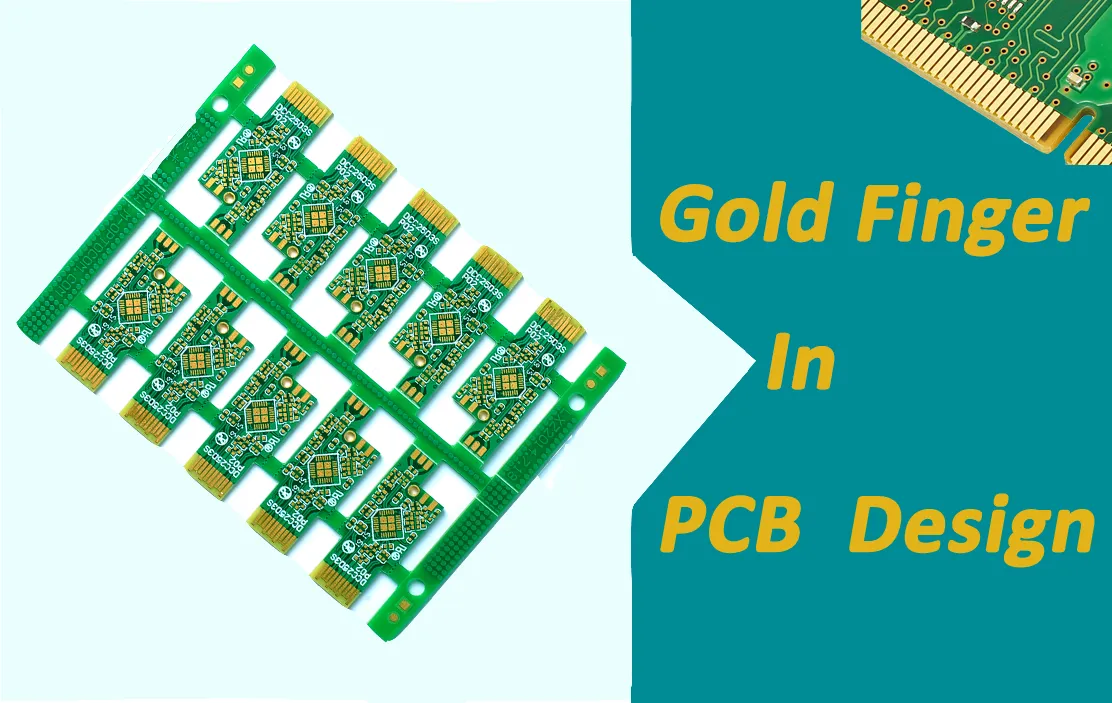
In modern electronics, where compactness, modularity, and high-speed signal transmission are crucial, printed circuit boards are engineered to not only host components but also serve as connectors. One prominent feature that enables interconnectivity is the gold finger. Found on the edges of PCBs, gold fingers are gold-plated connectors that slide into slots on other PCBs or devices, functioning similarly to USB connectors or expansion cards in computers.
This blog explores the role of gold fingers in PCBs, their design guidelines, applications, and industry best practices for manufacturing reliable and durable edge connectors.
What Are Gold Fingers?
Gold fingers are the plated edge connectors of a PCB, typically found on the edge of the board. These contacts are plated with a thin layer of hard gold (usually through an electrolytic process) over a nickel base. The term "fingers" refers to the visible, evenly spaced gold contacts that resemble the digits of a hand.
Gold fingers serve as the interface between a PCB and an external device. They provide high durability, excellent conductivity, and resistance to wear, making them ideal for applications requiring repeated insertion and removal.
Why Use Gold Plating?
Gold is used for plating PCB fingers because of its excellent electrical conductivity and strong resistance to corrosion and oxidation. The hardness of the gold layer (commonly 30-50 microinches) ensures the fingers can withstand repeated cycles of insertion without significant wear.
Nickel serves as an underlayer that provides structural integrity and acts as a barrier to prevent copper diffusion. Together, the nickel and gold layers form a durable, conductive, and corrosion-resistant interface.
Key Applications of Gold Fingers
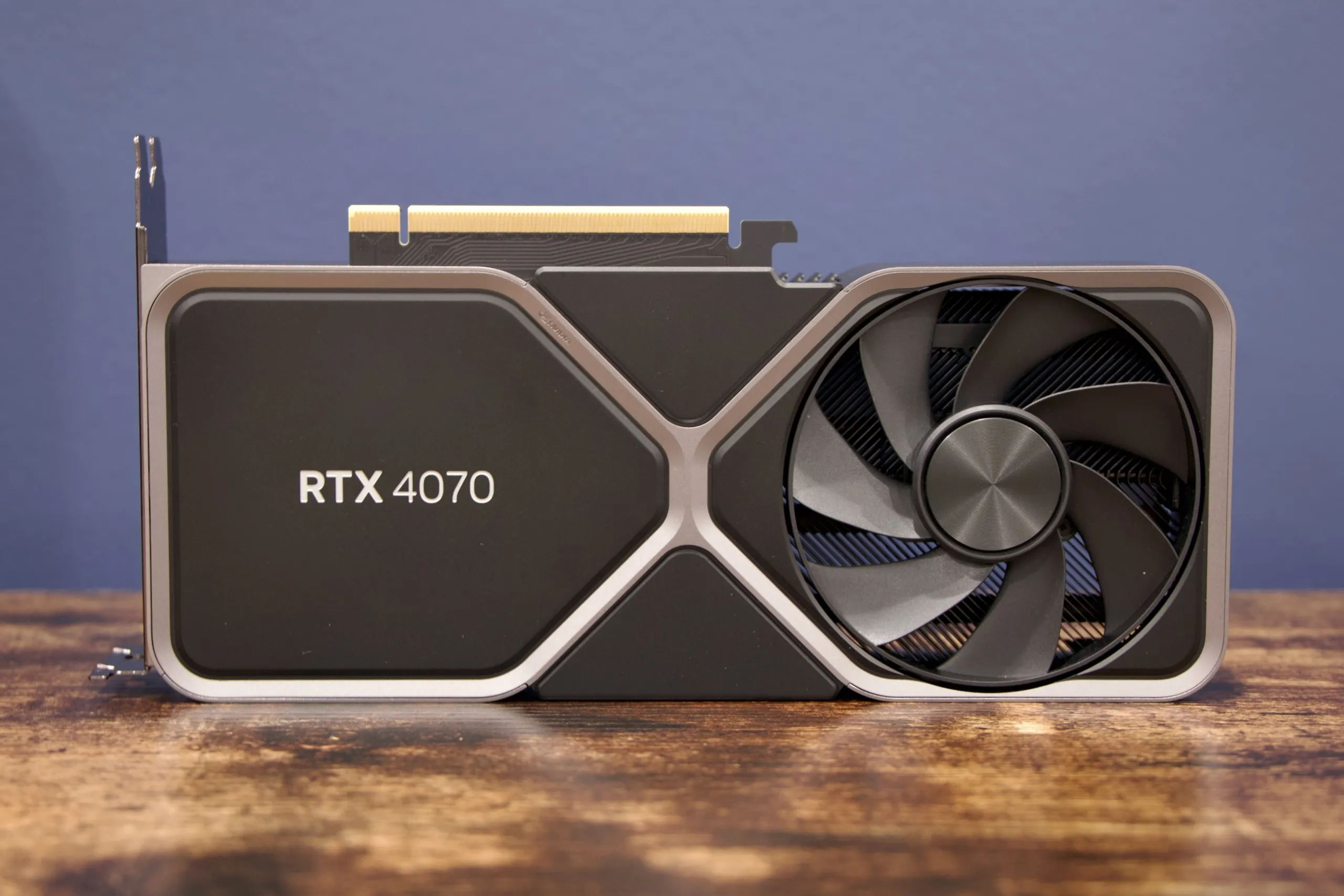
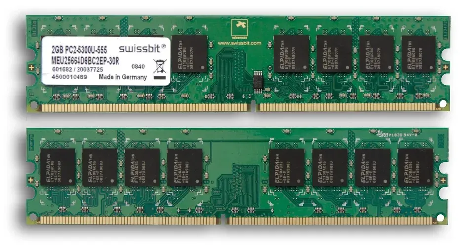
1.Computer and Server Motherboards: Gold fingers connect memory modules (e.g., RAM), GPUs, and peripheral devices.
2.Telecommunication Equipment: Used in routers, switches, and communication cards for fast, stable connections.
3.Medical Devices: In modular systems, allowing fast replacement and high reliability in critical applications.
4.Industrial Control Systems: Allow swappable control modules or interface boards.
5.Consumer Electronics: Devices like smartphones, gaming consoles, and cameras use edge connectors for modular assembly.
Design Guidelines for Gold Fingers
Designing gold fingers requires adherence to both mechanical and electrical specifications. Below are essential guidelines to follow:
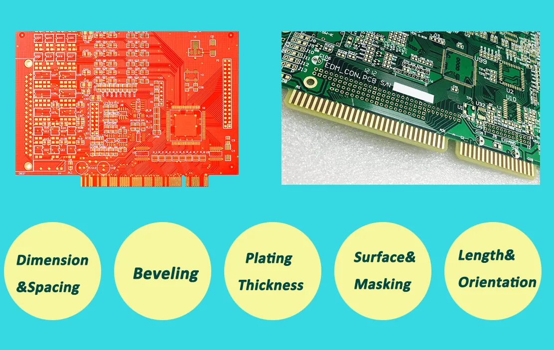
1. Finger Dimensions and Spacing
- Fingers must be uniformly spaced and aligned to match the slot connector.
- Typical finger width ranges from 1.0 mm to 3.5 mm.
- Spacing should allow proper insertion without physical interference.
2. Beveling (Chamfering)
- A bevel (usually 30 or 45 degrees) is applied to the edge of the PCB where gold fingers are located.
- Beveling ensures smooth insertion into a mating connector and reduces mechanical wear.
3. Plating Thickness
- Standard hard gold thickness is between 30 and 50 microinches.
- Some high-cycle applications may require up to 100 microinches.
4. Surface Preparation and Masking
- Gold fingers must be free of solder masks or silkscreen to ensure a clean contact surface.
- During manufacturing, fingers are masked off from other surface treatments like HASL or ENIG.
5. Length and Orientation
- Maintain consistent length to ensure equal pressure contact.
- Orientation should align with the slot connector to prevent damage during insertion.
Manufacturing Considerations
To manufacture reliable gold fingers, precise control of process parameters is critical. Key steps include:
- Nickel and Gold Plating: Electroplating is used to deposit nickel and then hard gold on the contact areas.
- Selective Masking: Only the finger area is plated with gold, while the rest of the board can use different surface finishes.
- Beveling: CNC routers or edge milling machines apply chamfers at precise angles.
Quality control measures such as thickness testing, adhesion testing, and surface smoothness checks are essential for ensuring performance and reliability.
Industry Standards
Compliance with industry standards ensures interoperability and quality. Some relevant standards include:
- IPC-A-600: Acceptability of Printed Boards
- IPC-6012: Qualification and Performance Specification for Rigid PCBs
- IPC-2221: Generic Standard on PCB Design
- IPC-4552: Specification for Electrodeposited and Electroless Nickel/Gold Coating
Adhering to these standards helps prevent quality issues such as finger misalignment, insufficient gold thickness, or surface contamination.
Common Mistakes to Avoid
1.No Beveling: Leads to difficult insertion and potential damage.
2.Insufficient Gold Thickness: Results in rapid wear and poor conductivity.
3.Contaminated Surface: Affects contact reliability and may lead to failures.
4.Incorrect Finger Spacing: This can cause insertion failure or connector damage.
Conclusion
Gold fingers are a vital element in PCB design, enabling modular connections and high reliability across a range of applications. Proper design and manufacturing, guided by industry standards, ensure long-lasting performance and signal integrity.
As demand for compact and high-speed devices increases, understanding gold finger design will be crucial for engineers, designers, and manufacturers alike.
Whether you're developing a cutting-edge communication system or a high-reliability medical device, applying best practices in gold finger implementation can significantly impact your product’s success.


