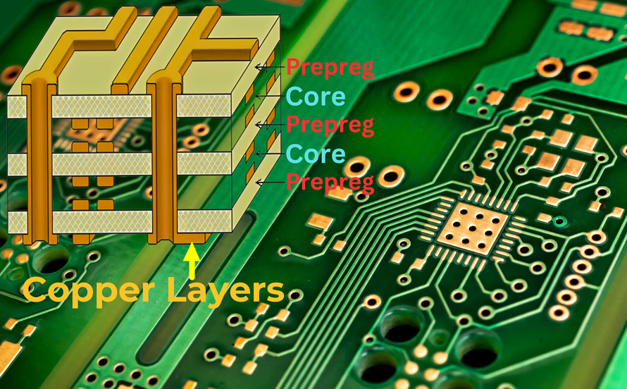
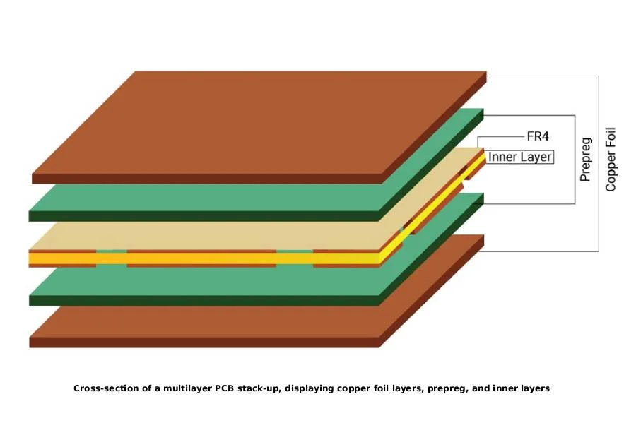
If you're wondering how copper pour affects PCB manufacturing costs, the answer lies in its dual role: it can both increase and decrease expenses depending on design choices and manufacturing processes. Copper pour, often used to improve signal integrity and thermal management, impacts material usage, production time, and overall board performance. In this detailed analysis, we'll explore how copper pour influences PCB costs, strategies for cost reduction, and ways to optimize copper utilization for efficient manufacturing.
What Is Copper Pour in PCB Design?
Copper pour, also known as copper flooding or copper fill, refers to the process of covering unused areas of a printed circuit board (PCB) with a layer of copper. This technique is commonly applied to ground or power planes to enhance electrical performance. By filling empty spaces on the board with copper, designers can reduce noise, improve heat dissipation, and provide a stable reference plane for signals.
However, while copper pour offers technical advantages, it also directly affects manufacturing costs. The amount of copper used, the complexity of the design, and the etching process all play a role in determining the final price of a PCB. Understanding these factors is key to balancing performance and budget.
How Copper Pour Impacts PCB Manufacturing Costs
The use of copper pour in PCB design has a significant effect on manufacturing expenses. Below, we break down the key ways it influences costs, focusing on material usage, production processes, and design complexity.
1. Increased Copper Material Usage
Copper is a primary material in PCB manufacturing, and its price fluctuates based on market conditions. When a design incorporates extensive copper pour, more copper foil is required to cover the board's surface. For instance, a typical 2-layer PCB with a 1 oz copper weight per square foot might see a cost increase of 10-15% if heavy copper pour is used across both layers, especially for larger boards.
Additionally, thicker copper layers (e.g., 2 oz or 3 oz) often used in power-intensive applications further drive up costs. While necessary for handling higher currents (up to 4A or more without overheating), this added material directly impacts the budget.
2. Etching and Fabrication Complexity
During PCB manufacturing, excess copper is etched away to create traces and patterns. With copper pour, less copper is removed, which might seem cost-effective at first. However, extensive copper pour can complicate the etching process by requiring precise control to avoid over-etching or under-etching, potentially increasing production time and costs. For complex designs with fine traces near poured areas, manufacturers may need specialized equipment or additional quality checks, adding to the expense.
3. Impact on Board Weight and Shipping
More copper means a heavier PCB. While this might seem minor, the added weight can increase shipping costs, especially for high-volume orders. For example, a batch of 1,000 boards with heavy copper pour could weigh significantly more than a batch with minimal copper, leading to higher logistics fees.
4. Thermal and Electrical Considerations
Copper pour is often used to manage heat and reduce electromagnetic interference (EMI). While this can lower costs indirectly by preventing design failures or the need for additional components (like heat sinks), poor implementation can lead to rework or scrap. For instance, uneven copper distribution might cause thermal stress during soldering, leading to board warping and costly production delays.
Strategies for PCB Cost Reduction with Copper Pour
While copper pour can increase manufacturing costs, there are ways to optimize its use for cost reduction without sacrificing performance. Below are actionable strategies to achieve this balance, focusing on efficient copper utilization in PCB design.
1. Optimize Copper Pour Coverage
Not every area of a PCB needs to be flooded with copper. By selectively applying copper pour only to critical areas, such as ground planes near high-speed signals or power traces, you can reduce material usage. For example, limiting copper pour to 50% of the board surface instead of 80% can cut copper costs proportionally while still maintaining adequate signal integrity (e.g., keeping impedance at 50 ohms for standard applications).
2. Use Standard Copper Weights
Choosing a standard copper weight, like 1 oz per square foot, instead of heavier options can significantly lower costs. Unless your design requires handling high currents or extreme thermal loads, sticking to lighter copper weights for pour areas is often sufficient. This approach reduces both material and processing expenses during fabrication.
3. Balance Copper Distribution
Uneven copper pour can lead to manufacturing issues like board warping during reflow soldering. To avoid costly rework, ensure copper distribution is balanced across layers. For a 4-layer PCB, aim for symmetrical copper coverage on outer and inner layers to minimize thermal stress. This not only reduces scrap rates but also improves yield, lowering overall production costs.
4. Collaborate Early with Manufacturers
Engaging with your PCB manufacturer during the design phase can uncover cost-saving opportunities related to copper pour. Manufacturers can provide feedback on optimal copper thickness, pour patterns, and panelization techniques to minimize waste. For instance, efficient panelization—arranging multiple PCBs on a single panel—can reduce material costs by up to 10%, especially when copper pour is factored into the layout.
Copper Utilization in PCB Design: Best Practices
Effective copper utilization in PCB design is crucial for balancing cost and performance. Here are best practices to ensure copper pour serves its purpose without unnecessarily inflating manufacturing expenses.
1. Prioritize Ground Planes for Copper Pour
Using copper pour primarily for ground planes is a cost-effective way to improve signal integrity. Ground planes help reduce noise in high-speed circuits (e.g., signals above 100 MHz) by providing a low-impedance return path. Focus copper pour on these areas rather than flooding non-critical sections of the board.
2. Avoid Overlapping Copper Pour with Traces
Overlapping copper pour with signal traces can create unintended capacitance, affecting signal timing and integrity. This might require redesigns or additional testing, driving up costs. Use design software to ensure proper clearance (e.g., 8 mils or more) between poured areas and traces to prevent such issues.
3. Incorporate Via Stitching with Copper Pour
For multilayer boards, via stitching—connecting copper pour across layers with vias—can enhance electrical and thermal performance. This technique ensures consistent grounding and heat distribution without excessive copper usage. For example, placing vias at 0.5-inch intervals around a ground plane can achieve effective EMI shielding without overfilling the board with copper.
4. Test and Validate Designs
Before finalizing a design with extensive copper pour, simulate and test for potential issues like thermal hotspots or signal interference. Thorough testing, including functional checks, can prevent costly recalls or redesigns. Allocate resources for validation to ensure copper pour adds value rather than creating problems.
Additional Factors Influencing PCB Copper Pour Costs
Beyond design and material choices, other factors related to copper pour can impact PCB manufacturing costs. Understanding these can help in making informed decisions.
1. Market Fluctuations in Copper Prices
Copper prices are subject to global market trends, and rising costs can directly affect PCB pricing. For instance, a 20% increase in copper prices over a year can translate to higher costs for boards with heavy copper pour. Staying updated on market conditions and planning production during stable price periods can mitigate this risk.
2. Manufacturing Scale and Volume
The cost impact of copper pour is more pronounced in small-batch production compared to high-volume runs. In large-scale manufacturing, the per-unit cost of copper usage decreases due to economies of scale. For small runs, consider minimizing copper pour to keep expenses in check.
3. Regional Manufacturing Differences
Manufacturing costs, including those influenced by copper pour, vary by region due to differences in labor, equipment, and material availability. Partnering with a manufacturer in a cost-effective region, while ensuring quality standards, can help manage expenses related to copper utilization.
Conclusion: Balancing Cost and Performance with Copper Pour
Copper pour plays a vital role in PCB design, offering benefits like improved signal integrity, reduced EMI, and better thermal management. However, its impact on manufacturing costs—through increased material usage, fabrication complexity, and logistics—cannot be overlooked. By optimizing copper pour coverage, using standard weights, balancing distribution, and collaborating with manufacturers, you can achieve significant cost reduction without compromising performance.
Effective copper utilization in PCB design is about making strategic choices. Focus on critical areas like ground planes, avoid unnecessary overlap with traces, and validate designs thoroughly to prevent costly errors. With these practices, you can harness the advantages of copper pour while keeping your PCB manufacturing budget in check.
Whether you're designing a simple 2-layer board or a complex multilayer PCB, understanding the cost implications of copper pour is essential. Implement the strategies discussed in this analysis to optimize your designs for both performance and affordability, ensuring your projects succeed in a competitive market.
 ALLPCB


