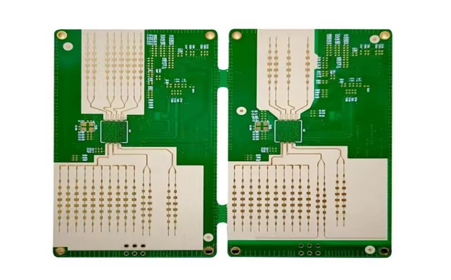
In the world of printed circuit board (PCB) design, managing heat is a critical challenge, especially for high-power applications. One innovative and effective approach is using the outer layer of a PCB as a heatsink. This technique can significantly improve heat dissipation and ensure the reliability of electronic components. In this comprehensive guide, we’ll explore how to leverage the outer layer for PCB thermal management, dive into various heat dissipation techniques, and provide actionable tips for high-power PCB designs. Whether you're looking for PCB heatsink design strategies or practical PCB cooling methods, this blog has you covered.
Why Thermal Management Matters in PCB Design
Heat is an inevitable byproduct of electronic components in operation. When current flows through resistors, transistors, or integrated circuits, it generates heat that can degrade performance, reduce lifespan, or even cause catastrophic failure if not managed properly. For high-power PCBs, where components often operate at elevated temperatures, effective thermal management is not just a luxury—it’s a necessity. Poor heat dissipation can lead to issues like thermal runaway, where components overheat and fail, costing time and resources to repair or replace.
Traditional cooling solutions, such as external heatsinks or fans, can add bulk and cost to a design. This is where using the PCB itself—specifically the outer layer—as a heatsink becomes a game-changer. By optimizing the board’s layout and materials, designers can achieve efficient cooling without relying heavily on external components.
What Does Using the Outer Layer as a Heatsink Mean?
The outer layer of a PCB refers to the top and bottom copper layers exposed to the environment. These layers can be used to dissipate heat by acting as a large thermal conductor that spreads heat away from hot components. By increasing the copper area on the outer layer and connecting it to heat-generating components through thermal vias or direct contact, the PCB can effectively transfer heat to the surrounding air or other cooling mechanisms.
This method is particularly useful for high-power PCB designs where space is limited, and adding external heatsinks isn’t feasible. It’s a cost-effective way to enhance PCB cooling methods while maintaining a compact form factor. However, to make this technique work, careful planning in the design phase is essential.
Benefits of Using the Outer Layer as a Heatsink
Before diving into the how-to, let’s look at why this approach is worth considering for your PCB heatsink design:
- Cost Efficiency: Utilizing the PCB’s existing copper layers reduces the need for additional cooling hardware, saving on material and assembly costs.
- Space Saving: For compact designs, using the outer layer eliminates the need for bulky external heatsinks or fans.
- Improved Reliability: Effective heat dissipation lowers component temperatures, extending their operational life and reducing failure rates.
- Simplified Assembly: Fewer external components mean a simpler manufacturing process, which can speed up production timelines.
Key Techniques for Effective PCB Thermal Management Using the Outer Layer
Now, let’s explore practical heat dissipation techniques and design strategies to maximize the outer layer’s potential as a heatsink. These methods are tailored for engineers looking to optimize PCB thermal management in high-power applications.
1. Maximize Copper Area on the Outer Layer
The simplest way to use the outer layer as a heatsink is to increase the copper surface area. Copper is an excellent conductor of heat, with a thermal conductivity of approximately 400 W/m·K. By dedicating large portions of the outer layer to copper pours (also called copper fills), you create a wider path for heat to spread out and dissipate into the air.
How to Implement: During layout design, allocate unused areas of the outer layer to copper pours connected to heat-generating components. Ensure these pours are not interrupted by traces or other elements that could restrict heat flow. For a component dissipating 5W of power, a copper area of at least 10-15 square inches on the outer layer can significantly lower its temperature by spreading the heat.
2. Use Thermal Vias for Heat Transfer
Thermal vias are small holes filled or plated with copper that connect the inner layers or components to the outer layer. They act as conduits, transferring heat from hot spots (like a power IC) to the outer copper layer for dissipation. Studies suggest that a grid of thermal vias with a diameter of 0.3mm and a spacing of 1.2mm can reduce component temperatures by up to 20°C in high-power designs.
How to Implement: Place an array of thermal vias directly under or near heat-generating components. Connect these vias to a large copper pour on the outer layer. Be mindful of via density—too many vias can weaken the board’s structural integrity, while too few may not transfer enough heat.
3. Optimize Component Placement
Where you place components on the PCB can make a big difference in thermal performance. Heat-generating components should be positioned near the edges of the board or in areas with direct access to large copper pours on the outer layer. This minimizes the distance heat must travel to reach the dissipating surface.
How to Implement: Group high-power components together and place them on one side of the board if possible. Avoid placing sensitive components, like microcontrollers, near these hot spots to prevent thermal interference. For example, a power MOSFET generating 8W of heat should be placed near a corner with a copper pour extending over 20 square inches for optimal cooling.
4. Choose the Right Board Material
The substrate material of your PCB plays a role in PCB thermal management. Standard FR-4 material has a thermal conductivity of about 0.3 W/m·K, which is relatively low. For high-power designs, consider using materials with better thermal properties, such as metal-core PCBs (MCPCBs), which can have thermal conductivities up to 10 W/m·K.
How to Implement: For applications exceeding 10W of power dissipation per square inch, opt for a metal-core board with an aluminum or copper base. This enhances the board’s ability to conduct heat to the outer layer, improving overall cooling efficiency.
5. Enhance Airflow Around the PCB
While the outer layer acts as a heatsink, its effectiveness depends on the surrounding environment. Heat dissipates faster in the presence of moving air. If the PCB is enclosed in a tight space with no ventilation, the heat will build up, negating the benefits of the outer layer design.
How to Implement: Design the enclosure with vents or slots to allow natural convection. If possible, incorporate small fans for forced airflow in high-power applications. Even a modest airflow of 100 linear feet per minute (LFM) can reduce PCB surface temperatures by 10-15°C.
Advanced Tips for High-Power PCB Cooling
For high-power PCB designs, where components might dissipate tens or even hundreds of watts, basic techniques may not be enough. Here are advanced strategies to take your PCB heatsink design to the next level.
1. Use Copper Thickness to Your Advantage
Standard PCBs often use 1oz copper (about 35 micrometers thick), which is fine for low-power applications. However, for high-power designs, increasing copper thickness to 2oz or even 3oz can improve thermal conductivity and current-carrying capacity. Thicker copper can reduce the thermal resistance of the outer layer, allowing it to handle more heat.
Practical Example: A 2oz copper layer can reduce the temperature rise of a power trace carrying 5A from 30°C to 15°C compared to a 1oz layer, assuming a 10mm wide trace.
2. Implement Heat Spreader Layers
In multilayer PCBs, internal copper layers can act as heat spreaders, distributing heat more evenly before it reaches the outer layer. This is especially useful when the outer layer alone cannot handle the thermal load.
How to Implement: Dedicate one or more internal layers to solid copper planes connected to thermal vias. This creates a larger thermal mass, reducing peak temperatures on the surface. For instance, an internal 1oz copper plane can lower component junction temperatures by up to 10°C in a 4-layer board design.
3. Consider Surface Finishes for Better Heat Radiation
The surface finish of the outer layer affects how well it radiates heat. Matte black finishes, for example, have higher emissivity (closer to 0.9) compared to shiny metallic finishes (emissivity around 0.1), meaning they radiate heat more effectively.
How to Implement: Choose a surface finish with high emissivity for the outer layer if radiation is a significant cooling mechanism in your design. Be aware, though, that this might slightly increase manufacturing costs.
Common Mistakes to Avoid in PCB Thermal Management
Even with the best intentions, it’s easy to make mistakes that undermine your PCB cooling methods. Here are pitfalls to watch out for:
- Insufficient Copper Area: Skimping on copper pours can limit heat dissipation, causing hot spots. Always allocate as much space as possible on the outer layer.
- Poor Via Placement: Placing thermal vias too far from heat sources reduces their effectiveness. Keep them close to the component’s thermal pad.
- Ignoring Airflow: Neglecting ventilation in the enclosure can trap heat, rendering the outer layer heatsink ineffective.
- Overloading the Outer Layer: For extremely high-power designs (above 50W), relying solely on the outer layer may not suffice. Combine this technique with other cooling solutions like external heatsinks.
Conclusion: Mastering Heat Dissipation in PCB Design
Using the outer layer as a heatsink is a powerful strategy for managing heat in PCB designs, especially for high-power PCB applications. By maximizing copper area, incorporating thermal vias, optimizing component placement, and enhancing airflow, you can create efficient PCB cooling methods that improve performance and reliability. These heat dissipation techniques not only save space and cost but also ensure your electronics operate within safe temperature ranges.
At ALLPCB, we’re committed to helping you achieve optimal PCB thermal management through innovative design and manufacturing solutions. Whether you’re working on a compact consumer device or a high-power industrial system, applying these PCB heatsink design principles can make all the difference. Start experimenting with these techniques in your next project, and watch your designs reach new levels of efficiency and durability.
 ALLPCB


