 ALLPCB


Are you struggling with smart home devices that fail too soon or underperform? The root cause often lies in the printed circuit board (PCB) design. In this detailed guide, we’ll uncover the top 5 design flaws that harm PCB reliability in smart home devices. From poor thermal management to signal integrity issues, we’ll explore each flaw, explain why it matters, and provide actionable tips to fix it. Whether you're an engineer or a product designer, this post will help you improve your smart home PCB design review process and boost device performance.
Why PCB Reliability Matters in Smart Home Devices
Smart home devices, like thermostats, security cameras, and smart lights, rely on PCBs to function seamlessly. These devices often operate 24/7 in varying conditions, making PCB reliability testing critical. A single design flaw can lead to overheating, signal loss, or complete failure, frustrating users and damaging your brand’s reputation. By addressing common design flaws, you can ensure longer device lifespans, better user experiences, and reduced manufacturing costs.
Let’s dive into the five major design flaws that could be undermining your smart home device’s PCB reliability and how to avoid them.
1. Poor Thermal Management in PCB Design
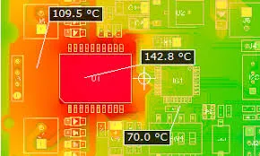
One of the biggest threats to PCB reliability in smart home devices is inadequate thermal management PCB design. Many smart home devices pack powerful processors and wireless modules into small enclosures, generating significant heat. If this heat isn’t dissipated properly, components can overheat, leading to performance drops or permanent damage.
For instance, a smart thermostat with a poorly designed PCB might see temperatures exceeding 85°C near critical components like microcontrollers. Most components are rated to operate safely below 70-80°C, so prolonged exposure to higher temperatures can reduce their lifespan by 50% or more.
How to Fix Thermal Management Issues
- Use Thermal Vias: Place thermal vias under heat-generating components like power regulators to transfer heat to other layers or a heat sink. A grid of 0.3mm vias spaced 1.2mm apart can significantly improve heat dissipation.
- Optimize Copper Planes: Dedicate larger copper areas on the PCB for heat spreading. A copper pour connected to ground can act as a passive heat sink.
- Choose the Right Materials: Use PCB substrates with higher thermal conductivity, such as FR-4 with enhanced thermal properties or metal-core PCBs for extreme cases.
- Simulate Heat Distribution: Before manufacturing, use thermal simulation tools to identify hotspots. Aim to keep component temperatures at least 10-15°C below their maximum ratings.
2. Signal Integrity Issues in Smart Home PCBs
Smart home devices often rely on high-speed signals for Wi-Fi, Bluetooth, or Zigbee communication. Signal integrity issues in smart home PCB design can cause data loss, connection drops, or erratic behavior. These issues arise from improper trace routing, impedance mismatches, or electromagnetic interference (EMI).
For example, a smart light bulb PCB with poorly routed high-speed traces might experience crosstalk, where signals interfere with each other. If a trace carrying a 2.4 GHz Wi-Fi signal is placed too close to another signal line without proper grounding, the error rate can spike, leading to unreliable performance.
How to Address Signal Integrity Problems
- Maintain Impedance Control: Design traces to match the impedance of your components, typically 50 ohms for RF signals. Use a controlled impedance calculator to determine trace width and spacing.
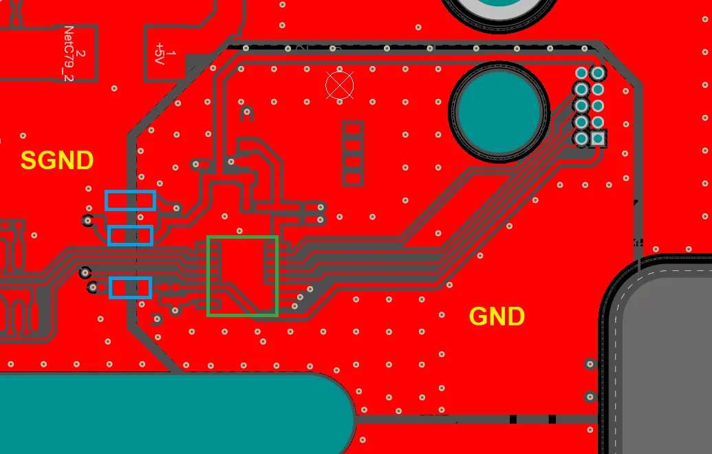
- Use Ground Planes: Place a continuous ground plane beneath high-speed signal traces to reduce EMI. Avoid splitting the ground plane unless absolutely necessary.
- Minimize Trace Lengths: Keep high-speed traces as short as possible to reduce signal delay and loss. For a 5 GHz signal, every 1mm of extra trace length can introduce measurable delay.
- Avoid Sharp Corners: Route traces with smooth, 45-degree bends instead of 90-degree angles to prevent signal reflection.
3. Incorrect Component Placement
Improper component placement guidelines are a common flaw in smart home PCB designs. Placing components without considering their interaction or environmental factors can lead to noise, heat buildup, or mechanical stress. For instance, placing a noise-sensitive sensor next to a power-hungry module can introduce interference, while clustering heat-generating components can create localized hotspots.
In a smart doorbell PCB, placing the Wi-Fi antenna near metal components or other RF sources can degrade signal strength by up to 30%, leading to dropped connections.
Best Practices for Component Placement
- Group by Function: Place components with similar functions together. For example, keep analog components away from digital circuits to minimize noise.
- Prioritize Heat Distribution: Spread out heat-generating components like voltage regulators or processors to avoid concentrated heat zones.
- Protect Sensitive Parts: Position sensitive components like sensors or RF modules away from sources of interference, such as switching power supplies.
- Consider Assembly: Ensure components are placed for easy soldering and inspection during manufacturing. Leave at least 2mm spacing between large components for accessibility.
4. Inadequate Power Distribution Design
A poorly designed power distribution network (PDN) can wreak havoc on smart home device reliability. Voltage drops, noise in the power lines, or insufficient current delivery can cause components to malfunction or fail. This is especially critical in smart home devices with multiple subsystems, such as a security camera with both image processing and wireless communication.
For example, if a PCB’s power traces are too narrow, they might not handle the current demand of a high-power module, leading to a voltage drop from 5V to 4.2V. Many microcontrollers require a stable 4.5-5V input, so this drop could trigger unexpected resets or crashes.
Tips for Better Power Distribution
- Widen Power Traces: Use wider traces for power and ground to handle higher currents. A trace width of 0.5mm can carry about 1A safely, but double it for higher loads.
- Add Decoupling Capacitors: Place decoupling capacitors (e.g., 0.1μF ceramic) close to each IC’s power pins to filter out noise. Position them within 2mm of the pin for best results.
- Use Power Planes: Dedicate an entire layer to power distribution if possible. This ensures low resistance and stable voltage across the board.
- Test Under Load: During PCB reliability testing, simulate real-world power demands to check for voltage drops or overheating in the PDN.
5. Lack of Proper Testing and Validation
Even a well-designed PCB can fail if it isn’t thoroughly tested. Skipping or rushing PCB reliability testing often results in undetected flaws that surface only after deployment. For smart home devices, which must operate reliably in diverse environments, testing for thermal stress, signal integrity, and power stability is non-negotiable.
For instance, a smart speaker PCB might pass basic functionality tests but fail under prolonged high-temperature conditions (e.g., 40°C for 48 hours). Without stress testing, such issues remain hidden until customers report failures.
Essential Testing Methods for PCB Reliability
- Thermal Cycling Tests: Expose the PCB to temperature extremes (e.g., -20°C to 85°C) over multiple cycles to check for component or solder joint failures.
- Signal Integrity Analysis: Use an oscilloscope to measure signal quality under different operating conditions. Look for overshoot, undershoot, or jitter in high-speed signals.
- Power Stress Testing: Operate the PCB at maximum load for extended periods to identify weaknesses in the power distribution network.
- Environmental Testing: Simulate real-world conditions like humidity (up to 85% RH) or vibration to ensure the PCB can withstand daily use in a smart home setting.
How to Conduct a Smart Home PCB Design Review
Before sending your PCB for manufacturing, a thorough smart home PCB design review can catch potential flaws early. Follow these steps to ensure your design is robust and reliable:
- Check Thermal Design: Verify that heat dissipation strategies are in place and simulate temperature profiles.
- Validate Signal Routing: Ensure high-speed traces are optimized and free from interference risks.
- Review Component Layout: Confirm that placement adheres to best practices for noise reduction and heat distribution.
- Inspect Power Delivery: Look for adequate trace widths, capacitor placement, and power plane usage.
- Plan for Testing: Define a testing protocol to validate the design under real-world conditions.
Investing time in a detailed design review can save you from costly recalls or redesigns down the line.
Conclusion: Build Reliable Smart Home Devices with Better PCB Design
Designing a reliable PCB for smart home devices is no small task, but avoiding these top 5 design flaws can make a huge difference. By focusing on thermal management PCB design, addressing signal integrity issues in smart home PCB, following component placement guidelines, optimizing power distribution, and committing to thorough PCB reliability testing, you can create devices that last longer and perform better.
Start with a comprehensive smart home PCB design review to spot issues early. With the right approach, your smart home devices will not only meet user expectations but also stand the test of time. At ALLPCB, we’re here to support you with expert resources and manufacturing solutions to bring your reliable designs to life.


