 ALLPCB


In the fast-evolving world of electronics, ensuring signal integrity in advanced printed circuit boards (PCBs) is more critical than ever, especially for high-frequency applications. One technique that plays a significant role in achieving this is controlled depth drilling. But what exactly is controlled depth drilling, and how does it impact signal integrity in advanced PCB design? Simply put, controlled depth drilling, often referred to as backdrilling, is a manufacturing process that removes unused portions of via stubs in through-hole vias, reducing signal loss and improving performance in high-frequency PCBs. In this blog, we’ll dive deep into the importance of controlled depth drilling, its effect on via stub effects, and how it contributes to signal loss reduction. Let’s explore this topic in detail to understand its role in modern PCB design.
What Is Controlled Depth Drilling in PCB Manufacturing?
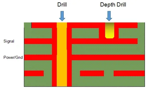
Controlled depth drilling, also known as backdrilling, is a precision manufacturing technique used in PCB fabrication. It involves drilling out the unused portion of a via after the initial through-hole plating process. Vias are small holes in a PCB that connect different layers of the board, allowing electrical signals to pass through. However, in high-frequency PCB designs, the unused part of a via, called a stub, can cause signal integrity issues by acting as an antenna that reflects signals.
By using controlled depth drilling, manufacturers can remove these stubs with high precision, leaving only the necessary portion of the via intact. This process minimizes signal reflections and interference, which are common challenges in advanced PCB designs operating at frequencies above 10 GHz. The result is a cleaner signal path, essential for applications like telecommunications, data centers, and high-speed computing.
Why Signal Integrity Matters in High-Frequency PCBs
Signal integrity refers to the ability of an electrical signal to travel through a PCB without distortion, noise, or loss. In high-frequency PCBs, where signals operate at speeds of several gigabits per second, maintaining signal integrity becomes a complex challenge. Issues like crosstalk, electromagnetic interference (EMI), and signal reflections can degrade performance, leading to data errors or system failures.
In such designs, even small imperfections can have a big impact. For instance, a via stub as short as 0.5 mm can cause significant signal reflection at frequencies above 5 GHz. This is where controlled depth drilling comes into play, directly addressing these problems by eliminating unnecessary via stubs and ensuring cleaner signal transmission.
The demand for high-speed electronics, such as those used in artificial intelligence (AI) chips and 5G technology, has made signal integrity a top priority. As frequencies increase, the margin for error decreases, making advanced techniques like controlled depth drilling indispensable.
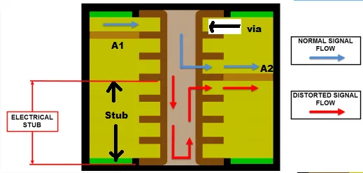
How Via Stub Effects Impact Signal Integrity
A via stub is the unused portion of a through-hole via that extends beyond the layer where a signal is routed. While this stub may seem harmless, it acts as a resonant structure in high-frequency PCBs. This resonance can cause signal reflections, leading to distortion and loss of data integrity. The longer the stub, the greater the impact on the signal, especially at higher frequencies.
For example, a via stub with a length of 1 mm can create a resonance at around 7.5 GHz, causing significant signal loss. This is a major concern in applications requiring high-speed data transfer, such as servers handling data rates of 25 Gbps or more. The reflection caused by the stub can result in impedance mismatches, further degrading the signal quality.
Controlled depth drilling directly tackles this issue by physically removing the stub, reducing the risk of resonance and reflections. This process ensures that the via only extends as far as needed, creating a smoother path for the signal to travel through the board.
The Role of Controlled Depth Drilling in Signal Loss Reduction
Signal loss is a critical concern in high-frequency PCB designs, as it directly affects the performance and reliability of electronic systems. Signal loss can occur due to various factors, including dielectric losses, conductor losses, and via stub effects. Controlled depth drilling specifically targets the loss caused by via stubs, offering a practical solution for signal loss reduction.
By removing the unused portion of the via, controlled depth drilling minimizes the capacitive and inductive effects that contribute to signal loss. Studies have shown that backdrilling can reduce signal loss by up to 20% in high-speed designs operating at 10 Gbps or higher. This improvement translates to better overall performance, especially in applications where every decibel of signal strength matters.
Additionally, controlled depth drilling helps maintain consistent impedance along the signal path. Impedance mismatches, often caused by via stubs, can lead to signal reflections and further loss. By eliminating stubs, this technique ensures a more uniform impedance, typically within a tolerance of ±10%, which is crucial for high-frequency signals.
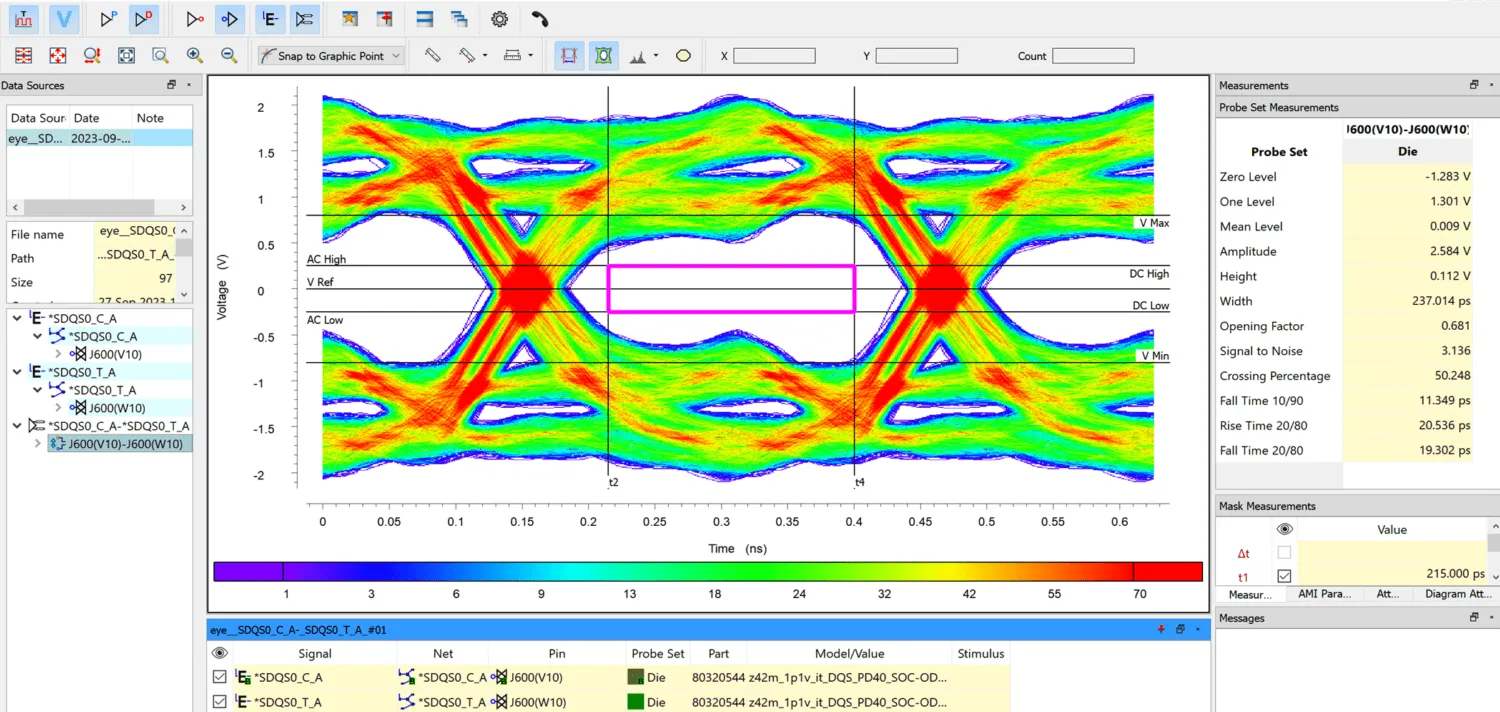
Controlled Depth Drilling Signal Integrity Analysis: How It Works
Conducting a controlled depth drilling signal integrity analysis is a vital step in advanced PCB design. This analysis involves simulating and testing the impact of backdrilling on signal performance using specialized software tools. Engineers can model the behavior of signals in a PCB layout, identifying potential issues caused by via stubs and determining the optimal depth for drilling.
During the analysis, key parameters such as signal rise time, impedance, and reflection coefficients are measured. For instance, a signal with a rise time of 100 ps (picoseconds) can be severely distorted by a via stub, leading to a reflection coefficient as high as 0.3. By simulating the effect of controlled depth drilling, designers can predict how removing the stub will improve these metrics, ensuring the signal remains intact.
This analysis also helps in fine-tuning the drilling process. Modern manufacturing equipment can achieve drilling depth tolerances as tight as ±0.05 mm, ensuring precision in stub removal without damaging the functional part of the via. The result is a PCB design optimized for high-frequency performance with minimal signal distortion.
Benefits of Controlled Depth Drilling in Advanced PCB Design
Controlled depth drilling offers several advantages for advanced PCB design, particularly in high-frequency applications. Here are some of the key benefits:
- Improved Signal Integrity: By eliminating via stubs, this technique reduces signal reflections and ensures cleaner signal transmission, critical for data rates above 10 Gbps.
- Reduced Signal Loss: Backdrilling minimizes capacitive and inductive losses, preserving signal strength over long traces and high frequencies.
- Enhanced Impedance Control: Removing stubs helps maintain consistent impedance, reducing mismatches that can degrade performance.
- Support for High-Speed Applications: Controlled depth drilling enables PCBs to handle the demands of modern technologies like 5G, AI, and high-performance computing.
- Cost-Effective Solution: While it adds a step to the manufacturing process, backdrilling can prevent costly redesigns by addressing signal integrity issues upfront.
These benefits make controlled depth drilling a go-to solution for engineers working on cutting-edge electronic systems where performance cannot be compromised.
Challenges and Considerations in Controlled Depth Drilling
While controlled depth drilling offers significant advantages, it also comes with challenges that must be addressed during the design and manufacturing stages. One primary concern is the precision required in the drilling process. If the drilling depth is not accurately controlled, it can damage the functional part of the via, leading to open circuits or unreliable connections.
Another consideration is the added cost and time in the manufacturing process. Controlled depth drilling requires specialized equipment and skilled operators, which can increase production costs by 10-15% compared to standard PCB fabrication. However, this cost is often justified by the performance gains in high-frequency designs.
Designers must also account for the limitations of backdrilling in densely populated boards. In some cases, the proximity of components and traces can make it difficult to apply controlled depth drilling without risking damage to nearby structures. Careful planning and simulation are essential to overcome these challenges.
Best Practices for Implementing Controlled Depth Drilling in PCB Design
To maximize the benefits of controlled depth drilling in advanced PCB design, engineers should follow these best practices:
- Simulate Early and Often: Use signal integrity analysis tools to model via stub effects and determine the optimal drilling depth before fabrication begins.
- Collaborate with Manufacturers: Work closely with your PCB fabrication partner to ensure they have the equipment and expertise needed for precise controlled depth drilling.
- Optimize Via Placement: Design your PCB layout to minimize the number of long vias and place them in areas accessible for backdrilling.
- Test Prototypes: Build and test prototypes with backdrilled vias to validate signal integrity improvements before full-scale production.
- Stay Updated on Standards: Follow industry standards for high-frequency PCB design, such as those from the Institute of Electrical and Electronics Engineers (IEEE), to ensure compliance and performance.
By adhering to these practices, you can seamlessly integrate controlled depth drilling into your design workflow, achieving superior signal integrity and performance.
Conclusion: The Future of Signal Integrity with Controlled Depth Drilling
As the demand for high-frequency PCBs continues to grow, techniques like controlled depth drilling are becoming essential tools in the engineer’s toolkit. By addressing via stub effects and contributing to signal loss reduction, this process plays a pivotal role in ensuring signal integrity in advanced PCB designs. Whether you’re working on cutting-edge telecommunications equipment or high-speed data systems, controlled depth drilling offers a reliable way to meet the stringent performance requirements of modern electronics.
Understanding the impact of controlled depth drilling on signal integrity is not just about improving current designs—it’s about preparing for the future. As frequencies climb higher and data rates increase, the precision and effectiveness of techniques like backdrilling will only become more critical. By embracing this technology and incorporating it into your design process, you can stay ahead in the ever-evolving world of PCB innovation.


