 ALLPCB


If you're looking to enhance the performance of your printed circuit board (PCB), understanding power plane stackup design is crucial. A well-optimized PCB layer stackup ensures better signal integrity, effective impedance control, and reliable power distribution. In this comprehensive guide, we'll dive into the essentials of optimizing stackup for signal integrity, stackup impedance control, and strategic power plane placement to help you achieve top-tier performance in your designs.
What Is Power Plane Stackup and Why Does It Matter?
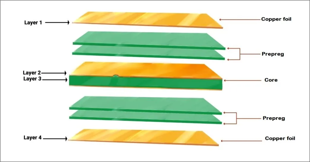
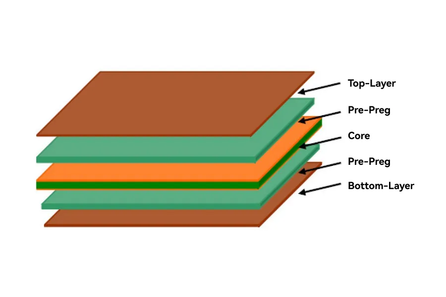
A power plane stackup refers to the arrangement of layers in a multi-layer PCB, specifically focusing on the placement of power and ground planes alongside signal layers. These planes are essential for providing stable voltage levels and a low-impedance return path for signals, which directly impacts the board's performance. A poorly designed stackup can lead to issues like electromagnetic interference (EMI), signal crosstalk, and power delivery problems, while a well-thought-out PCB layer stackup can significantly boost efficiency and reliability.
In modern electronics, where high-speed signals and compact designs are the norm, optimizing stackup for signal integrity and stackup impedance control becomes even more critical. Whether you're working on a 4-layer board for a simple device or a 12-layer board for a complex system, the principles of power plane stackup design remain the same: balance power distribution, minimize noise, and ensure consistent signal performance.
Key Principles of PCB Layer Stackup Design
Before diving into specific configurations, let’s explore the foundational principles that guide power plane stackup design. These principles will help you make informed decisions for any project, regardless of complexity.
1. Symmetry in Layer Arrangement
Symmetry in a PCB stackup is vital for manufacturing stability and performance. A symmetrical stackup prevents warping during fabrication by balancing the distribution of copper and dielectric materials. For instance, in a 4-layer board, a common configuration might include two signal layers on the outer sides and power and ground planes in the middle. This setup not only ensures mechanical stability but also aids in power plane placement for noise reduction.
2. Proximity of Power and Ground Planes
Placing power and ground planes close to each other creates a natural capacitance that helps filter out high-frequency noise. This close proximity reduces loop inductance, which is critical for maintaining a stable power delivery network (PDN). For high-speed designs, a separation of 3 to 5 mils (0.003 to 0.005 inches) between power and ground planes is often recommended to achieve optimal decoupling.
3. Signal Layer Placement for Integrity
Signal layers should be placed adjacent to a reference plane (either power or ground) to provide a consistent return path. This is a key aspect of optimizing stackup for signal integrity. Without a nearby reference plane, high-speed signals can suffer from crosstalk or EMI, leading to data errors. For example, in a 6-layer PCB, you might sandwich signal layers between ground planes to shield them from interference.
Common PCB Layer Stackup Configurations
Let’s look at some widely used PCB layer stackup configurations and how they incorporate power plane placement to optimize performance. Each configuration is tailored to specific needs, from basic designs to high-speed applications.
4-Layer PCB Stackup
The 4-layer stackup is one of the most common configurations for cost-effective designs that still require decent performance. A typical arrangement is:
- Layer 1: Top Signal
- Layer 2: Ground Plane
- Layer 3: Power Plane
- Layer 4: Bottom Signal
This setup ensures that signal layers have immediate access to a reference plane, aiding in stackup impedance control. The ground plane on Layer 2 acts as a shield, reducing EMI between the top and bottom signal layers. For a board handling signals up to 100 MHz, this configuration often provides sufficient performance with a controlled impedance of around 50 ohms for critical traces.
6-Layer PCB Stackup
For designs requiring more routing space or higher signal integrity, a 6-layer stackup offers additional flexibility. A common configuration is:
- Layer 1: Top Signal
- Layer 2: Ground Plane
- Layer 3: Inner Signal
- Layer 4: Inner Signal
- Layer 5: Power Plane
- Layer 6: Bottom Signal
This stackup allows for more complex routing while maintaining power plane placement close to signal layers for better noise suppression. It’s ideal for mixed-signal designs where analog and digital signals need separation to avoid interference.
8-Layer and Beyond
For high-speed or high-density designs, 8-layer or even 12-layer stackups are often necessary. These configurations provide dedicated planes for multiple voltage levels and additional shielding. A typical 8-layer stackup might look like this:
- Layer 1: Top Signal
- Layer 2: Ground Plane
- Layer 3: Signal
- Layer 4: Power Plane (3.3V)
- Layer 5: Power Plane (5V)
- Layer 6: Signal
- Layer 7: Ground Plane
- Layer 8: Bottom Signal
Here, multiple power planes cater to different voltage requirements, while ground planes provide shielding and return paths. This setup is excellent for optimizing stackup for signal integrity in applications like telecommunications or data processing, where signal speeds can exceed 1 GHz.
Optimizing Stackup for Signal Integrity
Signal integrity is a top concern in modern PCB design, especially as signal speeds increase. A poorly designed stackup can lead to signal degradation, crosstalk, or timing issues. Here’s how to ensure optimizing stackup for signal integrity through careful planning.
Minimize Crosstalk with Proper Layer Spacing
Crosstalk occurs when signals on adjacent layers interfere with each other. To prevent this, maintain adequate spacing between signal layers or use ground planes as shields. For high-speed signals (above 500 MHz), a dielectric thickness of 4 to 6 mils between layers can help reduce coupling while maintaining a controlled impedance of 50 ohms.
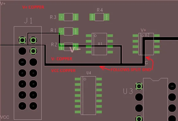
Use Continuous Reference Planes
Ensure that power and ground planes are continuous and not split unnecessarily. Splits in planes can disrupt the return path for signals, leading to noise and EMI. If a split is unavoidable, use stitching capacitors near the split to provide a high-frequency return path.
Stackup Impedance Control Techniques
Impedance control is essential for ensuring that high-speed signals travel without reflection or loss. Achieving stackup impedance control requires careful selection of materials and layer thickness.
Choosing the Right Dielectric Material
The dielectric constant (Dk) of the material between layers affects impedance. For standard FR-4 material, the Dk is typically around 4.2 to 4.5. For high-speed designs, consider low-Dk materials like Rogers 4350B (Dk around 3.5) to achieve tighter impedance control, often within ±10% of the target value (e.g., 50 ohms for single-ended traces).
Calculating Layer Thickness
Impedance is also influenced by the distance between a signal trace and its reference plane. Use an impedance calculator to determine the optimal dielectric thickness. For example, a 50-ohm trace on a 4-layer board might require a dielectric thickness of 8 mils between the signal layer and ground plane, assuming a trace width of 5 mils.
Best Practices for Power Plane Placement
Strategic power plane placement is critical for effective power distribution and noise reduction. Here are some best practices to follow:
Place Power Planes Near High-Current Components
Position power planes close to components that draw significant current, such as processors or FPGAs. This minimizes voltage drops and ensures stable power delivery. For instance, in an 8-layer board, dedicate a power plane near the top layers if high-power components are placed there.
Use Decoupling Capacitors Effectively
Decoupling capacitors placed near power pins help filter out noise and stabilize voltage. Use a mix of capacitor values (e.g., 0.1 μF and 10 μF) to cover a wide frequency range. Place these capacitors as close as possible to the power pins, ideally within 100 mils, to reduce inductance.
Challenges in Power Plane Stackup Design
While designing a power plane stackup, you may encounter challenges that require careful consideration. Addressing these issues upfront can save time and improve performance.
Balancing Cost and Performance
Adding more layers improves signal integrity and power distribution but increases manufacturing costs. For budget-conscious projects, a 4-layer or 6-layer stackup often strikes a good balance. Evaluate your design requirements to determine if additional layers are justified.
Managing Thermal Dissipation
Power planes can generate heat, especially in high-current applications. Ensure adequate copper thickness (e.g., 1 oz or 2 oz per square foot) on power planes to handle current without overheating. Additionally, consider vias or thermal pads to dissipate heat from power-intensive areas.
Conclusion: Building Better PCBs with Optimized Stackup Design
Designing an effective power plane stackup is a critical step in creating high-performance PCBs. By focusing on PCB layer stackup, optimizing stackup for signal integrity, achieving stackup impedance control, and mastering power plane placement, you can significantly enhance the reliability and efficiency of your designs. Whether you're working on a simple 4-layer board or a complex multi-layer system, these principles and configurations provide a roadmap to success.
Start by analyzing your project’s specific needs—signal speed, power requirements, and budget constraints—and apply the strategies discussed here to build a stackup that delivers. With careful planning and attention to detail, your PCB designs will stand out for their performance and durability.


