 ALLPCB


In the fast-paced world of electronics, multi-layer PCBs are the backbone of high-performance devices. But how do you ensure multi-layer PCB signal integrity in your designs? This guide from ALLPCB dives deep into the essentials of maintaining signal quality, tackling challenges like signal loss, crosstalk, and impedance control. Whether you're working on high-speed designs or complex circuits, this blog will equip you with practical strategies for success.
Signal integrity is critical in multi-layer PCBs to prevent data errors, delays, and performance issues. By mastering concepts like controlled impedance multi-layer PCB design and crosstalk reduction in multi-layer PCB, you can create reliable and efficient boards. Let’s explore the key principles, best practices, and actionable tips to optimize your designs for peak performance.
What Are Multi-Layer PCBs and Why Does Signal Integrity Matter?
Multi-layer PCBs consist of multiple layers of conductive material separated by insulating layers, allowing for compact and complex circuit designs. These boards are essential in modern electronics, from smartphones to industrial equipment, due to their ability to handle high-density connections and intricate routing.
However, with more layers and higher speeds, maintaining multi-layer PCB signal integrity becomes a challenge. Signal integrity refers to the quality of an electrical signal as it travels through the PCB. Poor signal integrity can lead to data corruption, timing errors, and electromagnetic interference (EMI). For high-speed multi-layer PCB design, ensuring signal integrity is non-negotiable to meet performance standards and avoid costly redesigns.
Key Challenges in Multi-Layer PCB Signal Integrity
Designing a multi-layer PCB for optimal signal integrity involves addressing several challenges. Let’s break down the most common issues and their impact on performance.
1. Signal Loss in Multi-Layer PCB
Signal loss in multi-layer PCB occurs when a signal weakens as it travels through the board, often due to resistance, dielectric losses, or skin effect at high frequencies. This loss can degrade performance, especially in high-speed applications where signals operate at gigahertz frequencies.
For example, at 5 GHz, a signal can lose up to 20% of its amplitude over a 10-inch trace if not designed properly. To minimize loss, use low-loss dielectric materials with a dielectric constant (Dk) below 3.5 and ensure shorter trace lengths. Additionally, smooth copper surfaces reduce skin effect losses at high frequencies.
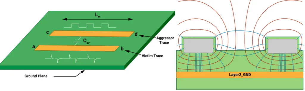
2. Crosstalk in Multi-Layer PCB
Crosstalk happens when signals on adjacent traces interfere with each other, causing noise and data errors. In multi-layer boards, tight spacing and parallel traces increase the risk of crosstalk reduction in multi-layer PCB becoming a priority.
To combat crosstalk, maintain a minimum spacing of 3x the trace width between high-speed signals. Using ground planes between signal layers also acts as a shield, reducing electromagnetic coupling. For instance, a 4-layer PCB with a dedicated ground plane can reduce crosstalk by up to 30% compared to a design without one.
3. Impedance Mismatches
In controlled impedance multi-layer PCB designs, maintaining consistent impedance is crucial for signal integrity. Impedance mismatches can cause reflections, leading to signal distortion. For high-speed signals like USB 3.0, a target impedance of 90 ohms differential is common, and deviations beyond ±10% can cause significant issues.
Use impedance calculators during design to match trace width, spacing, and dielectric thickness to the desired value. Stack-up planning, where signal layers are placed close to reference planes, helps achieve tighter control over impedance.
Best Practices for High-Speed Multi-Layer PCB Design
Designing for high-speed multi-layer PCB design requires a focus on layout, material selection, and routing techniques. Below are proven strategies to ensure signal integrity in your projects.
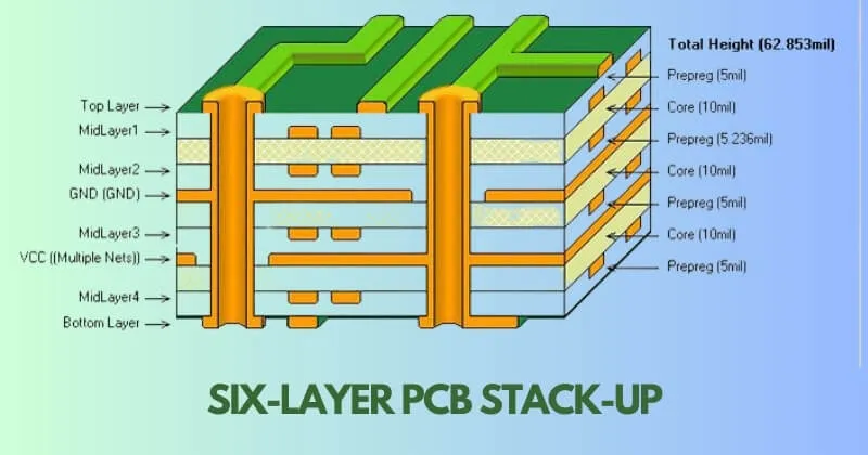
1. Optimize PCB Stack-Up for Signal Integrity
The arrangement of layers in a multi-layer PCB, known as the stack-up, plays a vital role in signal quality. A well-planned stack-up minimizes noise and supports controlled impedance.
For a 6-layer PCB, a common stack-up might be:
- Layer 1: Top Signal
- Layer 2: Ground Plane
- Layer 3: Inner Signal
- Layer 4: Power Plane
- Layer 5: Ground Plane
- Layer 6: Bottom Signal
Placing ground planes adjacent to signal layers provides a low-impedance return path, reducing EMI. Keep high-speed signals on outer layers or near reference planes to control impedance within ±5% of the target value.
2. Use Controlled Impedance Techniques
For controlled impedance multi-layer PCB designs, precise trace geometry and dielectric properties are essential. High-speed signals, such as those in DDR4 memory (operating at 3200 MT/s), often require a characteristic impedance of 50 ohms for single-ended traces.
Work with your PCB manufacturer to select materials with consistent dielectric constants (Dk between 3.0 and 4.0 for most high-speed applications). Use simulation tools to verify impedance before fabrication, as even a 0.1 mm variation in trace width can shift impedance by 5 ohms or more.
3. Minimize Signal Loss with Material Selection
Choosing the right materials can significantly reduce signal loss in multi-layer PCB designs. Standard FR-4 materials have a higher loss tangent (around 0.02), which can degrade signals at frequencies above 1 GHz. Instead, opt for advanced laminates with a loss tangent below 0.005 for better performance.
Additionally, consider copper foil with low roughness to minimize skin effect losses. These materials, while more expensive, can improve signal amplitude by up to 15% over long traces in high-frequency designs.
4. Implement Crosstalk Reduction Strategies
Effective crosstalk reduction in multi-layer PCB involves both layout and routing techniques. Avoid running high-speed traces parallel for long distances. If unavoidable, increase spacing or insert a ground trace between them to act as a barrier.
In a 10-layer board, dedicate inner layers to ground and power planes to isolate signal layers. This approach can reduce crosstalk-induced noise by up to 40%, ensuring cleaner signals in dense designs.
Advanced Tips for Multi-Layer PCB Signal Integrity
Beyond the basics, fine-tuning your design with advanced techniques can further enhance performance. These tips are especially useful for engineers working on cutting-edge applications.
1. Use Via Stubs Wisely
In multi-layer boards, vias connect traces between layers, but long via stubs can act as antennas, causing reflections. Back-drilling, a process to remove unused via stubs, can reduce signal reflections by up to 25% in high-speed designs operating above 10 Gbps.
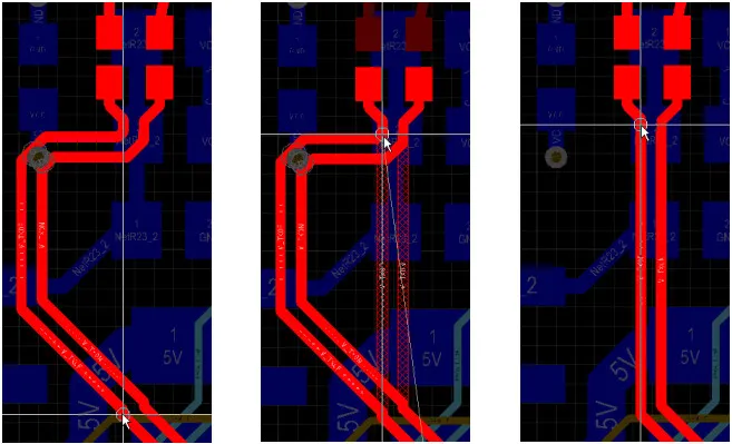
2. Implement Differential Pair Routing
For high-speed signals like PCIe or HDMI, differential pairs are common. Route these pairs with equal length and consistent spacing to maintain signal timing. A mismatch of just 5 mils (0.127 mm) can introduce skew, leading to data errors at speeds above 5 Gbps.
3. Simulate and Test Designs
Before manufacturing, use simulation software to model signal behavior. Tools can predict impedance mismatches, crosstalk, and signal loss, allowing you to tweak the design. Post-fabrication testing with a time-domain reflectometer (TDR) can verify impedance values within ±5% accuracy.
Common Mistakes to Avoid in Multi-Layer PCB Design
Even experienced engineers can overlook critical details. Here are pitfalls to steer clear of when focusing on multi-layer PCB signal integrity.
- Ignoring Ground Planes: Skipping continuous ground planes disrupts return paths, increasing EMI and signal noise.
- Overloading Layers: Routing too many high-speed signals on a single layer can lead to crosstalk and impedance issues.
- Neglecting Material Specs: Using standard materials for high-frequency designs often results in excessive signal loss in multi-layer PCB.
How ALLPCB Supports Your Multi-Layer PCB Needs
At ALLPCB, we understand the complexities of designing multi-layer boards for high-speed applications. Our advanced manufacturing capabilities ensure tight tolerances for controlled impedance multi-layer PCB designs, with impedance control within ±8%. We also offer a range of low-loss materials to minimize signal loss in multi-layer PCB projects.
Our team provides stack-up consultation and design review services to help you achieve optimal signal integrity. With fast turnaround times and rigorous quality checks, we’re committed to bringing your high-performance designs to life.
Conclusion: Building Better Multi-Layer PCBs
Mastering multi-layer PCB signal integrity is a game-changer for creating reliable, high-performance electronics. By focusing on high-speed multi-layer PCB design, addressing signal loss in multi-layer PCB, and prioritizing crosstalk reduction in multi-layer PCB, you can overcome common challenges and deliver exceptional results.
Start with a solid stack-up, choose the right materials, and apply best practices for routing and impedance control. With these strategies and support from ALLPCB, your multi-layer PCB projects will meet the demands of even the most complex applications. Let’s build the future of electronics together.


