ALLPCB


In the fast-paced world of electronics, high-speed designs demand precision and performance. One key technique that stands out for improving signal integrity is PCB edge plating. But how exactly does PCB edge plating enhance signal integrity in high-speed designs? Simply put, it creates a conductive layer along the edges of a printed circuit board (PCB), which helps reduce electromagnetic interference (EMI), improves grounding, and enhances thermal management—all critical factors for maintaining signal quality at high frequencies.
In this comprehensive guide, we’ll dive deep into the benefits of PCB edge plating for signal integrity, especially in high-frequency applications. Whether you’re an engineer working on cutting-edge technology or a designer looking to optimize your next project, this blog will provide actionable insights into how PCB edge plating can elevate your designs. Let’s explore the details behind this powerful technique and why it’s a game-changer for high-speed electronics.
What Is PCB Edge Plating and Why Does It Matter?
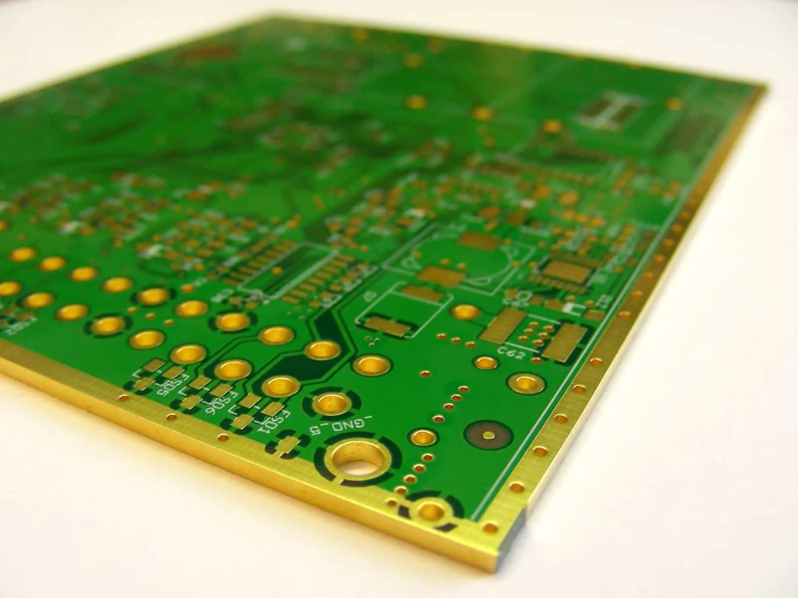
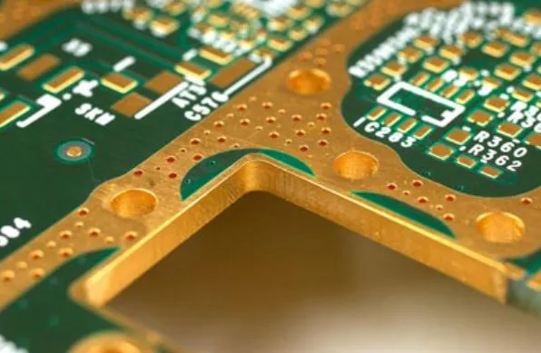
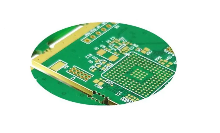
PCB edge plating, also known as board edge plating or castellation, is a manufacturing process where a conductive metal layer, typically copper, is applied along the perimeter or specific edges of a PCB. This plating connects the top and bottom layers of the board through the edge, creating a continuous conductive path. While it’s often used for mechanical strength or to facilitate soldering in modular designs, its impact on signal integrity in high-speed and high-frequency applications is significant.
In high-speed designs, signals travel at incredible speeds—often in the range of gigahertz (GHz)—and any disruption, such as noise or interference, can degrade performance. PCB edge plating addresses these challenges by providing better grounding and shielding, which are essential for maintaining clean signals. It’s particularly useful in applications like telecommunications, aerospace, and advanced computing, where even a small signal distortion can lead to major issues.
The Role of Signal Integrity in High-Speed Designs
Signal integrity refers to the quality of an electrical signal as it travels through a PCB. In high-speed designs, maintaining signal integrity is crucial because signals are more susceptible to issues like crosstalk, reflection, and EMI. These problems can cause data errors, timing issues, or complete system failures.
For instance, in a 5 GHz signal, even a slight impedance mismatch can cause reflections that distort the waveform. Impedance mismatches often occur at discontinuities, such as ungrounded edges or poorly designed traces. This is where PCB edge plating comes into play. By creating a uniform conductive boundary, it minimizes these discontinuities and helps maintain consistent impedance, typically in the range of 50 ohms for many high-speed applications.
Signal integrity isn’t just about speed—it’s also about reliability. Poor signal quality can lead to higher bit error rates (BER), which are unacceptable in critical systems like medical devices or automotive electronics. Understanding how to improve signal integrity is a priority for any engineer working on high-frequency designs, and PCB edge plating offers a practical solution.
How PCB Edge Plating Enhances Signal Integrity
Let’s break down the specific ways PCB edge plating contributes to signal integrity improvement in high-speed designs. Each of these benefits addresses a common challenge in high-frequency environments, making edge plating a valuable tool for engineers.
1. Reducing Electromagnetic Interference (EMI)
EMI is a major concern in high-speed designs because it can disrupt signals and cause interference between components. PCB edges, if left unplated, can act as antennas, radiating or picking up unwanted electromagnetic waves. This is especially problematic in densely packed boards where components are close together.
PCB edge plating helps by creating a grounded conductive shield along the board’s perimeter. This shield absorbs or redirects EMI, preventing it from affecting sensitive traces. For example, in a 10-layer PCB operating at 2.4 GHz for wireless communication, edge plating can reduce EMI by up to 20 dB, depending on the design and grounding strategy. This makes PCB edge plating EMI reduction a key reason to consider it for high-frequency projects.
2. Improving Grounding for Better Signal Return Paths
In high-speed designs, a proper ground plane is essential for providing a low-impedance return path for signals. Without a solid return path, signals can experience noise and distortion. Unplated PCB edges often create gaps in the grounding structure, forcing return currents to take longer, less efficient paths.
With PCB edge plating, the edges become part of the grounding system, creating a more uniform and continuous ground plane. This reduces ground bounce—a phenomenon where the ground voltage fluctuates due to high-speed switching—and ensures cleaner signals. For instance, in DDR4 memory designs operating at 3200 MT/s, edge plating can help stabilize ground potential, reducing noise by as much as 30% in some configurations.
3. Minimizing Signal Reflections at Board Edges
Signal reflections occur when a signal encounters a change in impedance, such as at the edge of a PCB. These reflections bounce back along the trace, interfering with the original signal and causing distortion. In high-frequency designs, where wavelengths are shorter, even small discontinuities at the board edge can trigger significant reflections.
PCB edge plating creates a consistent conductive boundary, reducing impedance mismatches at the edges. This helps signals terminate properly without bouncing back. For a 10 GHz signal, maintaining a controlled impedance of 50 ohms across the entire board, including the edges, is critical. Edge plating ensures that the signal sees a uniform environment, enhancing overall signal integrity.
4. Enhancing Thermal Management for High-Speed Components
High-speed components generate significant heat, which can affect signal integrity by altering the electrical properties of materials. Overheating can cause traces to expand or degrade, leading to impedance changes and signal loss. PCB edge plating aids in thermal management by providing an additional path for heat dissipation.
The plated edges act as a heat sink, drawing heat away from critical areas of the board. In a high-power RF amplifier design operating at 5 watts, edge plating can reduce edge temperatures by 5-10°C, depending on the board thickness and copper weight. This helps maintain stable signal performance over extended periods, making PCB edge plating high-frequency designs more reliable.
Design Considerations for Implementing PCB Edge Plating
While PCB edge plating offers clear benefits for signal integrity improvement, it’s important to implement it correctly to avoid potential pitfalls. Here are some practical design tips to ensure optimal results in high-speed and high-frequency applications.
1. Define Clear Edge Plating Areas
Not every PCB edge needs to be plated. Identify which edges are most critical for grounding or EMI shielding based on your design’s signal paths and component placement. Over-plating can increase manufacturing costs without providing additional benefits. For example, in a 4-layer PCB for a 1 GHz application, plating only the edges near high-speed traces may be sufficient.
2. Coordinate with Your Manufacturer
Edge plating requires precise manufacturing techniques, such as routing and plating processes, to ensure the conductive layer adheres properly. Work closely with your PCB fabrication team to specify the plating thickness—typically 1-2 ounces of copper—and ensure that the edges are free from burrs or defects that could affect signal integrity.
3. Balance Cost and Performance
While edge plating improves performance, it can add to the cost of PCB production due to the additional steps involved. Evaluate whether the benefits justify the expense for your specific project. For low-speed designs operating below 100 MHz, edge plating may not provide a significant advantage. However, for high-frequency designs above 1 GHz, the investment is often worthwhile.
4. Test and Validate Your Design
After implementing edge plating, use simulation tools to model signal integrity and EMI performance. Tools like time-domain reflectometry (TDR) can help measure impedance consistency along the board edges, ensuring that reflections are minimized. Real-world testing, such as eye diagram analysis for a 5 Gbps signal, can also confirm that edge plating is delivering the expected results.
Applications of PCB Edge Plating in High-Frequency Designs
PCB edge plating is particularly valuable in industries where high-frequency and high-speed designs are common. Here are a few examples of how it’s applied:
- Telecommunications: In 5G infrastructure, edge plating helps manage signals at frequencies up to 28 GHz, reducing EMI and ensuring reliable data transmission.
- Aerospace: Avionics systems operating at high frequencies benefit from edge plating to maintain signal integrity in harsh, noisy environments.
- Automotive: Advanced driver-assistance systems (ADAS) rely on high-speed radar signals, where edge plating minimizes interference for accurate sensor data.
- Consumer Electronics: Devices like high-speed gaming consoles use edge plating to support fast data rates, such as 8 Gbps for next-gen interfaces.
Challenges and Limitations of PCB Edge Plating
While PCB edge plating offers many advantages, it’s not without challenges. The additional manufacturing steps can increase production time, especially for complex multi-layer boards. There’s also a risk of shorts if the plating is not properly insulated from adjacent components or traces near the edge.
Moreover, edge plating may not be necessary for all designs. In lower-frequency applications or simpler boards, the cost and effort of edge plating may outweigh the benefits. Engineers must carefully assess their project requirements to determine if this technique aligns with their goals for signal integrity and performance.
Conclusion: Elevating High-Speed Designs with PCB Edge Plating
PCB edge plating is a powerful technique for improving signal integrity in high-speed and high-frequency designs. By reducing EMI, enhancing grounding, minimizing signal reflections, and aiding in thermal management, it addresses some of the most pressing challenges faced by engineers today. Whether you’re designing for telecommunications, aerospace, or consumer electronics, incorporating PCB edge plating can significantly boost the reliability and performance of your boards.
As technology continues to push the boundaries of speed and frequency, techniques like PCB edge plating will become even more critical. By understanding its benefits and implementing it thoughtfully, you can stay ahead in the competitive world of electronics design. With the right approach, PCB edge plating for signal integrity, high-frequency performance, and EMI reduction can transform your projects and deliver outstanding results.