 ALLPCB


In the rapidly evolving world of wearable technology, integrating sustainable power sources is a game-changer. Flexible solar PCBs (Printed Circuit Boards) offer a promising solution by combining lightweight, bendable designs with solar energy harvesting. However, designing and manufacturing these innovative components come with unique challenges. This blog dives deep into the intricacies of flexible solar PCB materials, wearable solar power PCB design, bending radius considerations, thin-film solar PCB assembly, and adhesive solutions for flexible solar PCBs. Whether you're an engineer or a tech enthusiast, you'll find practical insights to navigate these hurdles.
What Are Flexible Solar PCBs and Why Do They Matter for Wearable Technology?
Flexible solar PCBs are specialized circuit boards that integrate thin, bendable solar cells to power wearable devices like smartwatches, fitness trackers, and health-monitoring gadgets. Unlike traditional rigid PCBs, these boards can conform to the shape of the device or even the human body, making them ideal for compact, lightweight applications. Their ability to harness solar energy also reduces reliance on batteries, promoting eco-friendly and self-sustaining technology.
The importance of wearable solar power PCBs lies in their potential to revolutionize how we power personal electronics. With the wearable tech market projected to grow significantly, the demand for innovative power solutions is at an all-time high. However, creating these PCBs involves overcoming obstacles related to material selection, durability under bending stress, and efficient assembly processes. Let’s explore these challenges in detail.
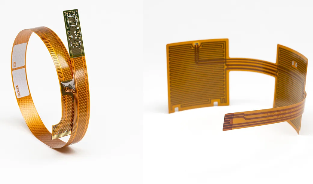
Key Materials for Flexible Solar PCBs: Balancing Durability and Performance
Choosing the right flexible solar PCB materials is critical to ensure both functionality and longevity. These materials must withstand repeated bending, resist environmental factors like humidity, and support efficient solar energy conversion. Common materials include:
- Polyimide (PI): Known for its excellent thermal stability and flexibility, polyimide is a popular substrate for flexible PCBs. It can handle temperatures up to 400°C, making it suitable for high-performance applications.
- Polyester (PET): A cost-effective option, PET offers good flexibility but is less resistant to high temperatures compared to polyimide. It’s often used in less demanding wearable devices.
- Thin-Film Solar Layers: Materials like amorphous silicon or perovskite are used for the solar cell layer. Perovskite, for instance, has shown efficiencies exceeding 20% in lab settings for flexible solar cells, even after thousands of bending cycles.
The challenge with these materials lies in balancing flexibility with electrical performance. For instance, while polyimide is durable, it can be more expensive, impacting production costs. Additionally, thin-film solar materials must maintain efficiency when bent or stretched, which requires careful integration into the PCB structure.
Design Challenges for Wearable Solar Power PCBs
Designing a wearable solar power PCB goes beyond simply embedding solar cells into a flexible substrate. Engineers must address several critical factors to ensure the PCB performs reliably in real-world conditions.
Optimizing Power Efficiency
Wearable devices often have limited surface area for solar cells, which means maximizing energy conversion efficiency is essential. Thin-film solar cells used in these PCBs typically achieve efficiencies between 10-20%, depending on the material and design. Engineers must strategically place solar cells to capture maximum sunlight without compromising the device's aesthetics or comfort.
Ensuring Comfort and Wearability
Since wearable devices are in direct contact with the skin, the PCB must be lightweight and non-intrusive. This requires minimizing the thickness of the board—often to less than 0.1 mm—while maintaining structural integrity. A poorly designed PCB can cause discomfort or skin irritation, driving users away from the product.
Environmental Durability
Wearable devices are exposed to sweat, humidity, and varying temperatures. Flexible solar PCBs must be designed with protective coatings to prevent corrosion or degradation of the solar cells. For example, encapsulating the solar layer with a moisture-resistant film can extend the lifespan of the PCB, even in humid conditions.
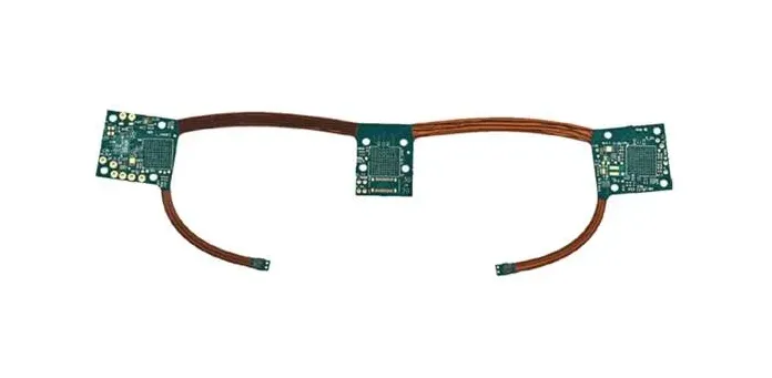
Bending Radius in Flexible PCBs: A Critical Design Consideration
The bending radius of a flexible PCB refers to the minimum radius at which the board can be bent without damaging its components or circuits. For wearable technology, where devices may need to curve around wrists or other body parts, understanding and optimizing the bending radius of flexible PCBs is crucial.
Typical bending radii for flexible PCBs range from 1 mm to 10 mm, depending on the material and thickness. A smaller bending radius allows for tighter curves but increases the risk of cracking or delamination. For instance, a polyimide-based PCB with a thickness of 0.05 mm can often achieve a bending radius as low as 1 mm, while thicker boards may require a larger radius to avoid stress fractures.
The challenge lies in testing and validating the bending radius under repeated cycles. Wearable devices may be bent thousands of times during their lifespan. Recent advancements have shown that some flexible solar cells can endure over 10,000 bending cycles while retaining up to 96% of their initial efficiency. However, integrating these cells into a PCB without compromising conductivity or solar performance requires precise engineering.
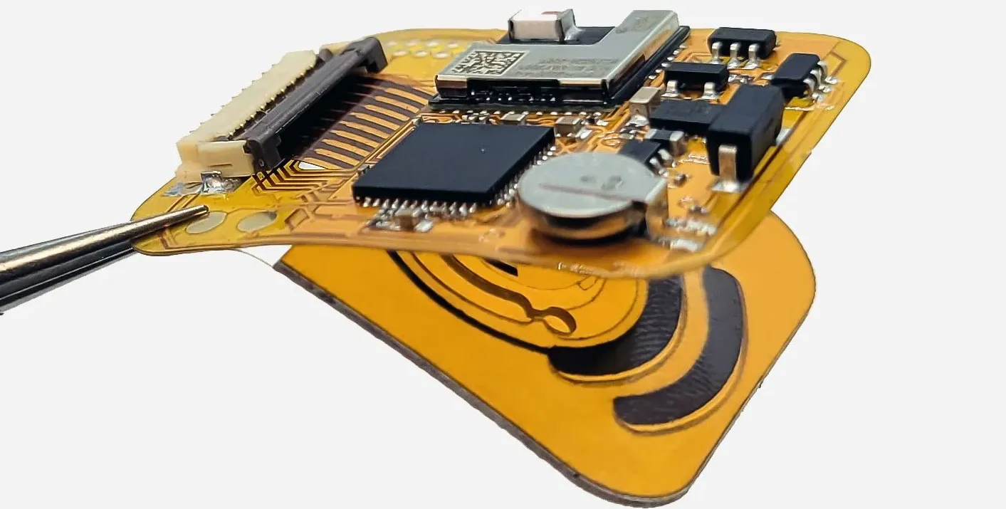
Manufacturing Challenges in Thin-Film Solar PCB Assembly
Assembling a thin-film solar PCB for wearable technology is a complex process that demands precision and innovation. Thin-film solar PCB assembly involves layering ultra-thin solar cells onto a flexible substrate, connecting them to conductive traces, and ensuring the entire structure remains functional under stress.
Precision in Layering and Alignment
Thin-film solar cells are often only a few micrometers thick, making them delicate to handle during assembly. Misalignment between the solar layer and the PCB’s conductive traces can lead to reduced efficiency or complete failure. Advanced manufacturing techniques, such as roll-to-roll processing, are often used to achieve the necessary precision at scale.
Thermal Management During Assembly
High temperatures during assembly can damage heat-sensitive solar materials. Traditional soldering, which often reaches temperatures of 600°F (316°C) or higher, is unsuitable for flexible solar PCBs. Instead, low-temperature bonding methods or conductive adhesives are preferred to maintain the integrity of the components.
Scalability and Cost
While thin-film solar technology offers flexibility, scaling production while keeping costs low remains a significant hurdle. The materials and processes involved, such as depositing solar layers via vacuum-based techniques, can be expensive. Finding cost-effective manufacturing solutions without sacrificing quality is a key focus for the industry.
Adhesive Solutions for Flexible Solar PCBs: Ensuring Reliability
Adhesives play a vital role in the construction of flexible solar PCBs, as they bond layers together while allowing flexibility and durability. Selecting the right adhesive for flexible solar PCBs is essential to prevent delamination or failure during bending.
Types of Adhesives
Conductive adhesives are often used instead of soldering to connect components in flexible PCBs. These adhesives contain conductive particles, such as silver or carbon, to maintain electrical connections. Non-conductive adhesives, on the other hand, are used for structural bonding and insulation, ensuring the layers of the PCB remain intact.
Key Properties of Adhesives
The ideal adhesive must be flexible, heat-resistant, and compatible with the materials used in the PCB. For instance, an adhesive with a tensile strength of at least 2 MPa can withstand the mechanical stress of bending. Additionally, it should cure at low temperatures (below 150°C) to avoid damaging sensitive solar cells.
Challenges in Adhesive Application
Applying adhesives uniformly across a flexible substrate is challenging, especially for ultra-thin PCBs. Uneven application can lead to weak spots or air bubbles, compromising the board’s performance. Advanced dispensing systems and curing techniques are often required to achieve consistent results.
Overcoming Design and Manufacturing Challenges: Best Practices
Navigating the complexities of flexible solar PCBs for wearable technology requires a combination of innovative design and manufacturing strategies. Here are some best practices to consider:
- Material Testing: Conduct thorough testing of flexible solar PCB materials under real-world conditions, including bending cycles and environmental exposure, to ensure durability.
- Simulation Tools: Use simulation software to model bending radius and stress points in the PCB design phase, reducing the risk of failure during production.
- Collaborative Design: Work closely with material suppliers and manufacturing teams to select cost-effective materials and processes that meet performance requirements.
- Iterative Prototyping: Build and test multiple prototypes to refine the design of wearable solar power PCBs, focusing on comfort, efficiency, and reliability.
Future Trends in Flexible Solar PCBs for Wearable Technology
The field of flexible solar PCBs is advancing rapidly, with exciting developments on the horizon. Innovations in materials, such as perovskite solar cells, promise higher efficiencies and greater flexibility. Additionally, advancements in manufacturing techniques, like 3D printing of conductive traces, could lower costs and improve scalability.
As wearable technology continues to evolve, the integration of flexible solar PCBs will likely become more seamless, enabling devices that are not only self-powered but also more comfortable and durable. Staying ahead of these trends will be crucial for engineers and manufacturers aiming to lead in this space.
Conclusion: Paving the Way for Sustainable Wearable Technology
Flexible solar PCBs hold immense potential to transform wearable technology by providing a sustainable and efficient power source. However, their design and manufacturing come with significant challenges, from selecting the right flexible solar PCB materials to optimizing bending radius and mastering thin-film solar PCB assembly. By addressing these hurdles with innovative solutions, such as advanced adhesives for flexible solar PCBs, the industry can unlock new possibilities for wearable devices.
At ALLPCB, we’re committed to supporting engineers and innovators in overcoming these challenges. With expertise in flexible PCB manufacturing and a focus on cutting-edge technology, we’re here to help bring your wearable solar power PCB designs to life. Explore our services to see how we can assist in creating the next generation of sustainable tech solutions.


