ALLPCB


If you're looking to reduce PCB assembly costs without compromising on quality, you've come to the right place. In this blog, we’ll explore six practical strategies to help you save money while ensuring your printed circuit boards (PCBs) meet high standards. From optimizing design elements to selecting cost-effective materials, these tips are tailored for engineers and manufacturers aiming to balance cost and performance. Let’s dive into the details of how you can achieve this, with a focus on key factors like PCB design elements influencing the cost of bare PCBs, layout count, via technology, size and shape, and surface finish.
Why PCB Assembly Costs Matter
PCB assembly is a critical step in electronics manufacturing, and its cost can significantly impact your project’s budget. High costs often stem from complex designs, expensive materials, or inefficient production processes. However, cutting corners can lead to poor performance, reliability issues, or even product failure. The goal is to find smart ways to lower expenses while maintaining the integrity of your design. By focusing on specific design and manufacturing choices, you can achieve substantial savings without sacrificing quality.

1. Optimize PCB Design for Manufacturability
One of the most effective ways to cut PCB assembly costs is to design with manufacturing in mind, often referred to as Design for Manufacturability (DFM). A well-thought-out design minimizes production challenges and reduces errors during assembly. Start by simplifying your layout to avoid unnecessary complexity. For instance, reducing the number of components or using standard sizes can lower both material and labor costs.
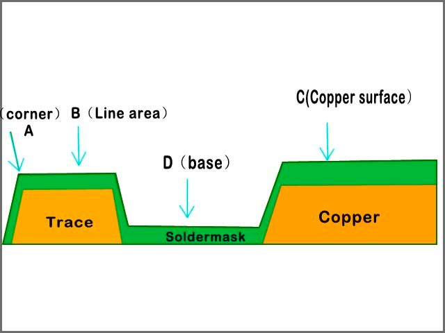
Pay attention to PCB design elements influencing the cost of bare PCBs, such as minimizing tight tolerances unless absolutely necessary. Tight tolerances often require specialized equipment or additional processing steps, driving up costs. Stick to industry-standard specifications wherever possible. Additionally, ensure your design files are clear and error-free to avoid costly revisions or delays during production.
Practical Tip: Use design software to run a DFM check before sending your files for manufacturing. Many assembly services offer free DFM analysis to catch potential issues early, saving you time and money.

2. Reduce Layer Count in Your PCB Layout
The layout count—or the number of layers in your PCB—directly affects the cost of bare PCBs. Each additional layer increases material usage, manufacturing time, and complexity, leading to higher expenses. While multi-layer boards are essential for complex circuits, consider whether your design truly requires extra layers. For simpler projects, a single-layer or double-layer board might suffice, significantly cutting costs.
For example, a 4-layer PCB might cost 30-50% more than a 2-layer board due to additional materials and processing. If your design can function with fewer layers by optimizing component placement and routing, you can achieve substantial savings. Always evaluate the trade-off between functionality and cost when deciding on the layer count.
Practical Tip: During the design phase, aim to consolidate signals and power planes into fewer layers. This not only reduces costs but also simplifies the assembly process.
3. Minimize Via Usage and Choose Cost-Effective Via Technology
Via technology plays a crucial role in PCB design, as vias create electrical connections between layers. However, the type and number of vias can significantly influence costs. Standard through-hole vias are generally the most affordable option, while advanced options like blind vias, buried vias, or microvias come with a higher price tag due to specialized manufacturing processes.
For instance, microvias, often used in high-density interconnect (HDI) boards, can increase costs by 20-40% compared to standard vias because of the precision required in drilling and plating. To save money, limit the number of vias in your design and avoid using advanced via types unless they’re critical to performance. Carefully plan your routing to reduce the need for vias while ensuring signal integrity.
Practical Tip: Use design tools to analyze via placement and explore alternative routing paths. Reducing via count by just 10-15% can lead to noticeable cost savings on larger production runs.

4. Standardize PCB Size and Shape for Efficiency
The size and shape of your PCB have a direct impact on manufacturing costs. Larger boards require more raw materials, while non-standard shapes (like circular or irregular designs) can lead to material waste and additional processing steps. To cut costs, aim for a rectangular or square shape that fits efficiently into standard panel sizes used by manufacturers, typically 18x24 inches or smaller.
For example, designing a PCB that maximizes panel utilization can reduce waste by up to 15-20%, lowering the per-unit cost. Avoid overly small boards as well, since they may require special handling during assembly, which can increase labor expenses. Stick to dimensions that align with your assembler’s equipment capabilities to avoid extra setup fees.
Practical Tip: Consult with your manufacturing partner early in the design process to understand their panelization guidelines. This ensures your PCB size and shape are optimized for cost-effective production.
5. Choose the Right Surface Finish for Cost and Performance
The surface finish of a PCB affects both its functionality and cost. Surface finishes protect the copper traces from oxidation and ensure good solderability during assembly. However, not all finishes are created equal in terms of expense. Options like Electroless Nickel Immersion Gold (ENIG) provide excellent performance but are more expensive due to the use of gold plating. On the other hand, Hot Air Solder Leveling (HASL), especially lead-free HASL, is a more budget-friendly choice for many applications.
For instance, ENIG can cost 10-30% more than HASL, depending on the board’s specifications. If your project doesn’t require high-frequency performance or extreme durability, opting for a cheaper finish like HASL can save money without affecting quality. Always match the surface finish to your project’s specific needs, such as environmental conditions or soldering requirements.
Practical Tip: If you’re unsure which finish to choose, discuss with your assembly provider. They can recommend a cost-effective option that meets your performance criteria.
6. Leverage Bulk Ordering and Long-Term Partnerships
Finally, consider the benefits of bulk ordering and building long-term relationships with your PCB assembly provider. Ordering in larger quantities often qualifies you for volume discounts, reducing the per-unit cost. For example, ordering 1,000 units instead of 100 might lower the cost per board by 10-25%, depending on the provider’s pricing structure.
Additionally, partnering with a reliable manufacturer for multiple projects can lead to better pricing, faster turnaround times, and improved communication. A trusted partner understands your needs and can offer tailored solutions to optimize costs without compromising quality. They may also provide value-added services like free design reviews or prototyping at a reduced rate.
Practical Tip: Plan your production schedule to combine smaller orders into a single larger run when possible. This approach maximizes savings and minimizes setup costs for the manufacturer.
Additional Cost-Saving Tips for PCB Assembly
Beyond the six main strategies, here are a few extra ways to trim expenses:
- Use Standard Components: Opt for widely available, off-the-shelf components instead of custom or rare parts. This reduces procurement costs and lead times.
- Minimize Manual Assembly: Design your PCB for automated assembly processes like surface-mount technology (SMT). Manual labor for through-hole components can increase costs by 15-20%.
- Avoid Over-Specification: Don’t specify higher-grade materials or tolerances than necessary. For example, using a standard FR-4 substrate instead of a high-frequency material can save up to 30% if your design doesn’t require special properties.

Balancing Cost and Quality: Key Takeaways
Reducing PCB assembly costs without sacrificing quality is entirely achievable with the right approach. By focusing on design optimization, reducing layer count, minimizing via usage, standardizing size and shape, selecting cost-effective surface finishes, and leveraging bulk orders, you can save significantly while maintaining high standards. Remember that every design decision impacts cost, so plan carefully and collaborate with your manufacturing partner to identify savings opportunities.
Pay special attention to PCB design elements influencing the cost of bare PCBs, such as layout count, via technology, size and shape, and surface finish. These factors are often the biggest drivers of expense, but they also offer the greatest potential for cost reduction when addressed thoughtfully.
Conclusion
Cutting PCB assembly costs doesn’t mean compromising on quality. With strategic design choices and smart manufacturing practices, you can achieve a balance that benefits both your budget and your product’s performance. Start by reviewing your current designs with these six strategies in mind, and don’t hesitate to reach out to your assembly provider for guidance. At ALLPCB, we’re committed to helping you navigate these challenges with tailored solutions that prioritize both cost and quality. Implement these tips in your next project, and watch your savings grow without sacrificing the reliability your customers expect.