 ALLPCB


In the fast-paced world of electronics, high-speed rigid-flex PCB design is critical for ensuring performance and reliability in compact, complex devices. Whether you're working on telecommunications equipment, medical devices, or consumer electronics, understanding the nuances of rigid-flex PCB design can make or break your project. So, what are the key considerations for designing a high-speed rigid-flex PCB? The top five factors include impedance control, signal integrity, crosstalk management, signal loss mitigation, and material selection. In this comprehensive guide, we'll dive deep into each of these aspects to help you create robust and efficient designs that meet high-speed requirements.
Why High-Speed Rigid-Flex PCB Design Matters
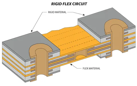
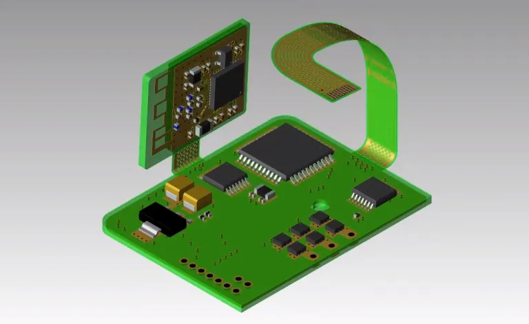
Rigid-flex PCBs combine the benefits of rigid and flexible circuits, offering durability and adaptability in a single board. They are ideal for high-speed applications where signals must travel quickly and accurately across different sections of a device. However, designing these boards for high-speed performance introduces unique challenges. Issues like signal degradation, interference, and impedance mismatches can disrupt functionality if not addressed early in the design process. By focusing on the five key considerations outlined below, you can optimize your high-speed rigid-flex PCB for peak performance and reliability.
1. Impedance Control in Rigid-Flex PCB Design
Impedance control is a cornerstone of high-speed rigid-flex PCB design. It ensures that signals travel along traces without reflections or distortions, which can degrade performance. In high-speed applications, maintaining a consistent characteristic impedance—often around 50 ohms for single-ended signals or 100 ohms for differential pairs—is crucial.
In rigid-flex designs, impedance control becomes more complex due to the transition between rigid and flexible sections. The dielectric materials and thicknesses often differ between these areas, affecting the impedance. To manage this, designers must carefully calculate trace widths and spacing using impedance calculators or simulation tools. For example, a trace width of 5 mils on a 1 oz copper layer with a dielectric constant (Dk) of 3.5 might achieve a 50-ohm impedance in the rigid section, but adjustments are needed in the flexible section where the Dk might be lower.
Best practices for rigid-flex PCB impedance control include using consistent stack-up designs, minimizing layer transitions, and selecting materials with stable dielectric properties. Additionally, avoid abrupt changes in trace geometry at the rigid-flex interface to prevent impedance mismatches.

2. Ensuring Signal Integrity in High-Speed Rigid-Flex PCBs
Signal integrity refers to the quality of an electrical signal as it travels through a PCB. In high-speed rigid-flex PCB designs, maintaining signal integrity is vital to prevent data loss or errors. Poor signal integrity can result from reflections, noise, or timing issues, especially when signals operate at frequencies above 1 GHz.
To ensure rigid-flex PCB signal integrity, start by minimizing trace lengths in high-speed signal paths. Shorter traces reduce the risk of signal degradation and delay. For instance, in a design operating at 5 Gbps, keeping differential pair traces under 5 inches can help maintain signal quality. Additionally, route high-speed signals on inner layers with solid ground planes to shield them from external noise.
Another critical factor is managing the bend radius in flexible sections. Tight bends can cause signal distortion due to changes in trace geometry. A minimum bend radius of 10 times the thickness of the flex layer is often recommended. Finally, use proper termination techniques, such as series or parallel termination resistors, to match impedance and reduce reflections.
3. Managing Crosstalk in Rigid-Flex PCB Layouts
Crosstalk is the unwanted coupling of signals between adjacent traces, which can interfere with data transmission in high-speed rigid-flex PCBs. This issue is particularly pronounced in dense layouts where traces are closely spaced to save space.
To mitigate rigid-flex PCB crosstalk, maintain adequate spacing between high-speed traces. A general rule of thumb is to keep spacing at least three times the width of the trace. For example, if a trace is 4 mils wide, ensure at least 12 mils of separation from neighboring traces. Differential pairs, often used in high-speed designs, should be routed closely together but kept away from other signal groups to avoid interference.
Ground planes play a significant role in reducing crosstalk. Placing a continuous ground plane beneath high-speed traces provides a return path for signals and acts as a barrier against electromagnetic interference (EMI). In flexible sections, where ground planes may be limited, consider using hatched ground patterns to maintain shielding without compromising flexibility.
4. Minimizing Signal Loss in High-Speed Rigid-Flex PCBs
Signal loss, or attenuation, occurs when a signal’s strength diminishes as it travels through a PCB. In high-speed rigid-flex PCB designs, signal loss can result from dielectric losses, conductor losses, or transitions between rigid and flexible sections. Excessive loss can lead to unreliable data transmission, especially at frequencies above 10 GHz.
Material selection is a primary factor in controlling rigid-flex PCB signal loss. Low-loss dielectrics, such as polyimide for flexible sections and high-frequency laminates for rigid areas, are essential. These materials have a lower dissipation factor (Df), often below 0.005, which reduces energy loss. For instance, using a laminate with a Df of 0.002 at 10 GHz can significantly improve signal performance compared to standard FR-4 with a Df of 0.02.
Conductor losses can be minimized by using smoother copper finishes, as rough surfaces increase resistance at high frequencies due to the skin effect. Additionally, avoid excessive vias in high-speed signal paths, as each via introduces insertion loss. If vias are unavoidable, use back-drilling techniques to remove unused via stubs that can cause signal reflections.
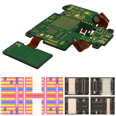
5. Material Selection and Stack-Up Design for Rigid-Flex PCBs
The choice of materials and stack-up design directly impacts the performance of high-speed rigid-flex PCBs. Unlike rigid-only boards, rigid-flex designs require materials that balance mechanical flexibility with electrical performance. This dual requirement makes material selection a critical consideration.
For flexible sections, polyimide is the most common material due to its excellent thermal stability and flexibility. It supports high-speed signals with dielectric constants typically ranging from 3.2 to 3.5. In rigid sections, high-frequency laminates with low dielectric constants and dissipation factors are preferred for minimizing signal loss and maintaining impedance control.
The stack-up design must ensure a smooth transition between rigid and flexible layers. A typical high-speed rigid-flex stack-up might include 6 to 8 layers, with high-speed signals routed on inner layers adjacent to ground planes. Use symmetrical stack-ups to prevent warping during manufacturing, and specify adhesive-less constructions for better reliability in flexible areas.
Thermal management is another factor to consider. High-speed circuits generate heat, which can affect material properties and signal performance. Incorporate thermal vias or heat sinks in rigid sections to dissipate heat effectively, ensuring long-term reliability.
Additional Tips for High-Speed Rigid-Flex PCB Design
Beyond the five key considerations, there are several practical tips to enhance your high-speed rigid-flex PCB designs. First, use simulation tools to model signal behavior before fabrication. Tools like SPICE or 3D electromagnetic simulators can predict impedance mismatches, crosstalk, and signal loss, allowing you to make adjustments early.
Second, collaborate closely with your manufacturing partner to ensure design rules align with their capabilities. Rigid-flex PCBs have unique manufacturing constraints, especially regarding bend areas and layer transitions. Clear communication can prevent costly redesigns.
Finally, test prototypes under real-world conditions. High-speed designs often behave differently in simulation versus actual operation due to environmental factors like temperature and humidity. Thorough testing ensures your design performs as expected in the field.
Conclusion: Mastering High-Speed Rigid-Flex PCB Design
Designing a high-speed rigid-flex PCB requires careful attention to detail and a deep understanding of electrical and mechanical principles. By focusing on impedance control, signal integrity, crosstalk management, signal loss mitigation, and material selection, you can create boards that meet the demands of modern high-speed applications. These five key considerations provide a roadmap for success, helping you avoid common pitfalls and achieve reliable, high-performance designs.
At ALLPCB, we understand the complexities of high-speed rigid-flex PCB design and are committed to supporting engineers with the tools and expertise needed to bring their ideas to life. Whether you're tackling a new project or refining an existing design, keep these principles in mind to ensure your rigid-flex PCB performs flawlessly in even the most challenging environments.


