 ALLPCB


Designing RF (Radio Frequency) PCBs is a specialized skill that demands precision and attention to detail. One of the most critical aspects of this process is RF PCB trace design, which directly impacts signal integrity and performance. If you're looking to master RF PCB trace width calculation, understand RF PCB trace impedance, follow RF PCB trace spacing rules, optimize RF PCB trace geometry, or enhance RF PCB trace design for signal integrity, you're in the right place. In this comprehensive guide, we'll break down the essentials of RF PCB trace design to help you create high-performing circuits for your high-frequency applications.
Why RF PCB Trace Design Matters
RF circuits operate at high frequencies, often in the range of hundreds of megahertz to several gigahertz. At these frequencies, even small design flaws in trace width, spacing, or geometry can lead to signal loss, interference, or impedance mismatches. Unlike low-frequency circuits, where traces act merely as conductive paths, RF traces behave as transmission lines, where electromagnetic fields and wave propagation play a significant role. A well-designed RF PCB trace ensures minimal signal distortion, reduced electromagnetic interference (EMI), and consistent performance.
Whether you're designing for wireless communication, radar systems, or IoT devices, mastering RF PCB trace design is essential. Let’s dive into the key elements—width, spacing, and geometry—and explore how to optimize them for the best results.

Understanding RF PCB Trace Width Calculation
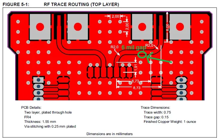
Determining the correct trace width is the foundation of RF PCB design. The width of a trace affects its current-carrying capacity, heat dissipation, and most importantly, its impedance. For RF applications, trace width is often calculated to achieve a specific characteristic impedance, typically 50 ohms for most RF systems, as this matches common RF components and test equipment.
To calculate the trace width for a desired impedance, you need to consider several factors, including the substrate material (like FR4 or Rogers), the dielectric constant (often denoted as εr, typically 4.2–4.6 for FR4), the thickness of the substrate, and the copper thickness. A widely used tool for this is an online impedance calculator or specialized PCB design software that uses formulas derived from transmission line theory.
For example, a microstrip line (a common RF trace type) on a standard FR4 substrate with a 1.6mm thickness and a target impedance of 50 ohms might require a trace width of approximately 2.8mm. However, this value can vary based on the exact material properties and design constraints. Adjusting the trace width slightly can fine-tune the impedance to prevent signal reflections that degrade performance.
Keep in mind that wider traces reduce resistance and can handle more current, but they may not fit in compact designs. Narrower traces, while space-efficient, risk higher resistance and potential overheating. Balancing these factors during RF PCB trace width calculation is key to a successful design.
Mastering RF PCB Trace Impedance
Impedance is a critical parameter in RF PCB design. RF PCB trace impedance determines how well a trace can transmit a signal without reflections or losses. Mismatched impedance between a trace and its connected components (like amplifiers or antennas) can cause signal reflections, leading to reduced power transfer and potential data errors.
The characteristic impedance of a trace depends on its width, the distance to the ground plane, and the dielectric properties of the PCB material. For instance, a 50-ohm impedance is standard for most RF applications because it minimizes losses in coaxial cables and matches most RF hardware. To achieve this, designers must carefully calculate and simulate the trace dimensions during the layout phase.
There are different types of transmission lines used in RF designs, such as microstrip (trace on the surface with a ground plane below) and stripline (trace sandwiched between two ground planes). Each type has unique impedance calculation formulas. For a microstrip, impedance decreases as trace width increases or as the distance to the ground plane decreases. Using high-frequency materials with a lower dielectric constant can also help maintain consistent impedance across frequencies, as standard FR4 materials may exhibit variations at higher frequencies (above 1 GHz).
Ensuring proper RF PCB trace impedance often requires simulation tools to account for real-world variables like manufacturing tolerances or frequency-dependent dielectric losses. A mismatch as small as 5 ohms can cause noticeable signal degradation in sensitive RF systems.
Following RF PCB Trace Spacing Rules
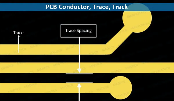
Trace spacing is another crucial factor in RF PCB design. RF PCB trace spacing rules help prevent crosstalk, reduce EMI, and maintain signal integrity. At high frequencies, adjacent traces can couple electromagnetically, leading to unwanted interference. Proper spacing minimizes this coupling and ensures that signals remain clean.
A general rule of thumb for RF trace spacing is to keep traces at least three times the trace width apart from each other. For example, if your trace width is 0.5mm, maintain a spacing of at least 1.5mm between parallel traces. This "3W rule" reduces crosstalk by keeping the electric and magnetic fields from overlapping significantly.
Additionally, spacing between traces and ground planes or other reference planes must be considered. Too little spacing can alter the impedance of the trace, while too much spacing can make the design unnecessarily large. In differential pair routing, often used in high-speed RF designs, maintaining consistent spacing between the pair (typically 2–3 times the trace width) ensures balanced signal transmission and minimizes noise.
Finally, avoid routing RF traces near high-speed digital signals or power lines, as these can introduce noise. If such routing is unavoidable, increase the spacing or use shielding techniques like guard traces connected to ground.
RF PCB Trace Geometry Optimization
The geometry of RF traces—beyond just width and spacing—plays a vital role in performance. RF PCB trace geometry optimization involves shaping and routing traces to minimize signal loss, avoid sharp corners, and maintain consistent impedance throughout the signal path.
One key aspect of geometry optimization is avoiding sharp 90-degree bends in traces. At RF frequencies, sharp corners can act as antennas, radiating energy and causing signal loss or interference. Instead, use 45-degree angles or smooth, curved bends to maintain signal integrity. For very high frequencies (above 5 GHz), even 45-degree bends may cause issues, and mitered or rounded corners are preferred.
Another consideration is trace length. In RF designs, the physical length of a trace can affect signal timing and phase, especially in applications like antenna matching networks or phased arrays. Keeping traces as short as possible reduces signal delay and losses. For instance, at 2.4 GHz (a common frequency for Wi-Fi), a wavelength in a typical PCB material is about 50mm. A trace longer than 1/10th of this wavelength (5mm) can start to exhibit transmission line effects, requiring careful impedance control.
Lastly, consider the placement of vias in RF traces. Vias introduce inductance and capacitance, which can disrupt impedance and cause signal reflections. If vias are necessary, use them sparingly and ensure they are surrounded by ground vias to minimize parasitic effects.
RF PCB Trace Design for Signal Integrity
Signal integrity is the ultimate goal of RF PCB trace design. RF PCB trace design for signal integrity focuses on ensuring that signals reach their destination without distortion, noise, or loss. Poor signal integrity can result in data errors, reduced range in wireless systems, or complete circuit failure.
To maintain signal integrity, start with a solid ground plane. A continuous, unbroken ground plane beneath RF traces provides a low-impedance return path for signals and reduces EMI. Avoid splitting the ground plane or routing traces over gaps, as this can create loops that act as antennas for noise.
Next, pay attention to impedance matching throughout the signal path. Any discontinuity in impedance—whether from a via, a connector, or a change in trace width—can cause reflections. Use matching networks (like LC circuits) or tapered traces to transition between different impedance values smoothly.
Decoupling capacitors near RF components are also essential. These capacitors filter out noise and stabilize power delivery, preventing voltage fluctuations from affecting signal quality. Place them as close as possible to the power pins of RF ICs, with short traces to minimize inductance.
Finally, simulate your design before fabrication. Modern PCB design tools allow you to model signal behavior at RF frequencies, identifying potential issues like crosstalk or impedance mismatches before they become costly mistakes. For example, a simulation might reveal that a 3mm trace segment near a via causes a 10% signal reflection, allowing you to adjust the layout accordingly.
Practical Tips for RF PCB Trace Design
Here are some actionable tips to refine your RF PCB trace design process:
- Choose the Right Material: High-frequency designs often benefit from specialized substrates with low dielectric loss, especially for frequencies above 1 GHz.
- Use Simulation Tools: Software with built-in RF simulation capabilities can predict impedance, signal loss, and crosstalk before manufacturing.
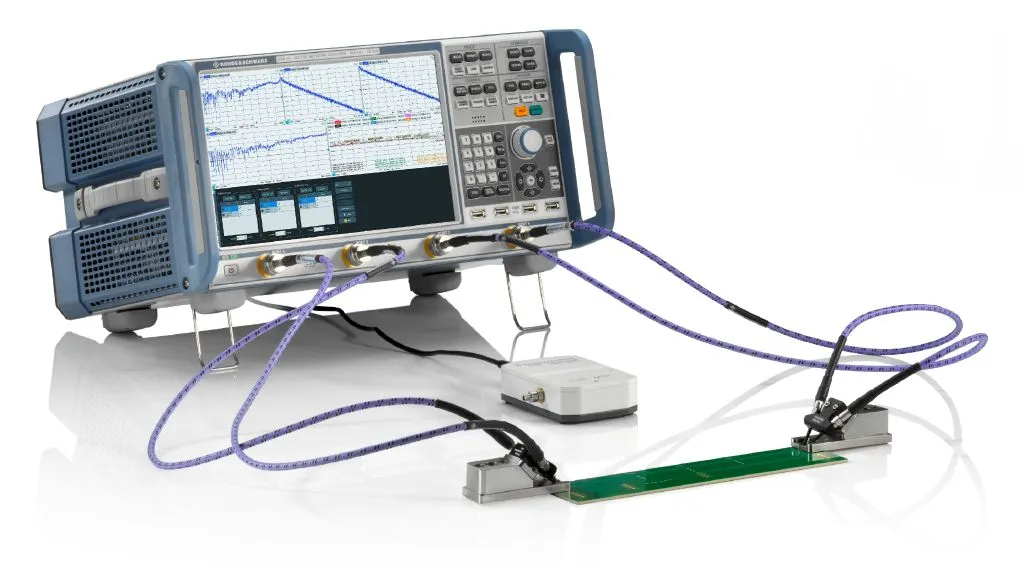
- Test and Iterate: After fabrication, use a vector network analyzer (VNA) to measure impedance and signal performance, then refine your design as needed.
- Minimize Layer Transitions: Keep RF signals on a single layer when possible to avoid vias and maintain consistent impedance.
- Follow Manufacturer Guidelines: Work closely with your PCB fabricator to understand their tolerances for trace width and spacing, as small deviations can impact RF performance.
Conclusion: Perfecting the Art of RF PCB Trace Design
RF PCB trace design is both a science and an art, requiring a deep understanding of width, spacing, geometry, impedance, and signal integrity. By mastering RF PCB trace width calculation, maintaining proper RF PCB trace impedance, adhering to RF PCB trace spacing rules, optimizing RF PCB trace geometry, and focusing on RF PCB trace design for signal integrity, you can create high-performing circuits for even the most demanding applications.
Every detail matters in RF design—from the width of a trace to the angle of a bend. With careful planning, simulation, and testing, you can ensure your RF PCB performs reliably at high frequencies. Whether you're a beginner or a seasoned engineer, these principles and tips will help you tackle the challenges of RF design with confidence.
Ready to bring your RF PCB project to life? Start applying these techniques in your next design and see the difference that precision makes.


