ALLPCB


In the world of PCB design, PCB trace spacing plays a critical role in ensuring a board's performance, reliability, and manufacturability. Striking the right balance between high-density layouts, minimizing crosstalk and signal coupling, and adhering to manufacturing limits can be challenging. This blog dives deep into the essentials of trace spacing, exploring key guidelines like the 3W rule and 5S rule, while addressing design for manufacturability (DFM), high-density interconnect (HDI) challenges, and safety considerations like clearance and creepage. Whether you're a seasoned engineer or just starting out, this guide will help you navigate these critical aspects of PCB design with practical insights and actionable tips.
What Is PCB Trace Spacing and Why Does It Matter?
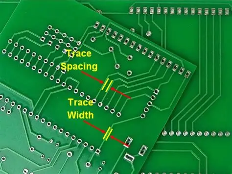
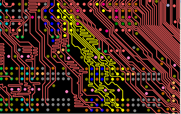
PCB trace spacing refers to the distance between conductive traces on a printed circuit board. This spacing directly impacts several factors, including electrical performance, signal integrity, and the overall safety of the board. Proper spacing prevents issues like crosstalk—unwanted electromagnetic interference between adjacent traces—and ensures that the board can be manufactured without defects.
In modern designs, especially with high-density interconnect (HDI) layouts, engineers often push for tighter spacing to fit more components into smaller areas. However, reducing spacing too much can lead to signal coupling, where signals interfere with each other, degrading performance. Additionally, spacing must comply with manufacturing constraints to avoid production errors and meet safety standards for clearance and creepage in high-voltage applications.
In this blog, we’ll break down the key considerations for trace spacing, provide guidelines to minimize interference, and explain how to align your design with manufacturing capabilities. Let’s get started with the fundamentals of trace spacing and its impact on PCB performance.
Understanding Crosstalk and Signal Coupling in PCB Design
Crosstalk is a common issue in high-speed and high-density PCB designs. It occurs when electromagnetic fields from one trace induce unwanted signals in a nearby trace, leading to noise and signal integrity problems. Signal coupling, a related phenomenon, happens when traces are too close, allowing signals to “couple” or interfere with each other through capacitive or inductive effects.
For high-speed signals, such as those running at 1 GHz or higher, crosstalk can distort waveforms, increase bit error rates, and cause system failures. The risk is especially high in densely packed boards where traces are routed close together to save space. To mitigate these issues, engineers must carefully plan trace spacing and routing strategies.
The 3W Rule: A Practical Solution for Crosstalk
One widely used guideline to reduce crosstalk is the 3W rule. This rule states that the spacing between two parallel traces should be at least three times the width of the traces. For example, if a trace is 5 mils wide, the spacing between it and the next trace should be at least 15 mils. This increased distance helps minimize electromagnetic coupling by reducing the strength of the interfering fields between traces.
The 3W rule is particularly effective for high-speed digital signals, where maintaining signal integrity is critical. However, it may not always be feasible in HDI designs where space is limited. In such cases, additional strategies like using ground planes or guard traces can complement the 3W rule to further suppress interference.
The 5S Rule: Enhancing Signal Integrity
Another useful guideline is the 5S rule, which focuses on spacing relative to the signal’s rise time and propagation speed. While less commonly discussed than the 3W rule, the 5S rule suggests maintaining a spacing that ensures signals on adjacent traces do not interfere within five times the signal’s rise time. This is especially relevant for very high-speed designs where timing is critical, such as in DDR memory interfaces operating at speeds above 2.5 Gbps.
By adhering to these spacing rules, designers can significantly reduce the risk of crosstalk and signal coupling, ensuring reliable performance even in complex layouts.
Balancing Trace Spacing with High-Density Interconnect (HDI) Designs
In high-density interconnect (HDI) designs, the push for smaller board sizes and more components often leads to reduced trace spacing. HDI technology enables finer traces (as small as 3 mils) and tighter spacing (down to 3 mils in some cases), allowing for compact layouts in devices like smartphones and wearables. However, this comes with challenges in maintaining signal integrity and meeting manufacturing limits.
For HDI boards, trace spacing must be carefully calculated to avoid crosstalk while ensuring the design can be produced without defects. Most manufacturers have minimum spacing requirements based on their fabrication capabilities—often around 4-6 mils for standard processes. Pushing below these limits can result in manufacturing errors like short circuits or incomplete etching.
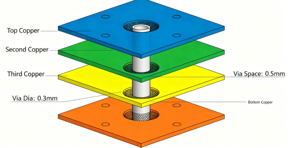
To succeed with HDI designs, engineers should collaborate closely with their PCB fabrication partners to understand specific design for manufacturability (DFM) guidelines. Using advanced routing techniques, such as microvias and buried vias, can also help achieve dense layouts without sacrificing spacing or performance.
Clearance and Creepage: Safety in High-Voltage Designs
Beyond signal integrity, trace spacing is critical for safety in high-voltage PCB designs. Two key terms to understand are clearance and creepage. Clearance refers to the shortest distance between two conductive elements through the air, while creepage is the shortest distance along the surface of an insulating material between those elements.
Inadequate clearance or creepage can lead to arcing or electrical breakdown, posing risks of fire or equipment damage. Standards like IPC-2221 provide guidelines for minimum clearance and creepage distances based on voltage levels, environmental conditions, and pollution degrees. For example, at 500V, a typical clearance requirement might be 8 mm in a clean environment, while creepage could be slightly higher to account for surface contamination.
Designers working on high-voltage boards must prioritize these safety distances over density considerations. This often means increasing trace spacing beyond what’s needed for signal integrity, especially in industrial or medical applications where reliability is non-negotiable.
Manufacturing Constraints: Aligning Design with Production Capabilities
While optimizing PCB trace spacing for performance and safety is essential, designs must also align with manufacturing limits. Every PCB fabrication house has specific capabilities and constraints, often dictated by their equipment and processes. Common manufacturing limits for trace spacing typically range from 5 to 8 mils for standard boards, though advanced facilities can handle tighter tolerances.
Designing with design for manufacturability (DFM) in mind ensures that your board can be produced without costly delays or defects. For instance, spacing traces too closely can lead to issues like over-etching, where traces become thinner than intended, or under-etching, where excess copper causes shorts. To avoid these problems, always review the manufacturer’s DFM guidelines before finalizing your layout.
Additionally, consider the impact of fabrication tolerances on impedance control. For high-speed designs, trace width and spacing directly affect characteristic impedance (often targeted at 50 ohms for single-ended signals). A deviation of just 1 mil in spacing can shift impedance by several ohms, potentially causing signal reflection and loss. Using simulation tools to model these effects during the design phase can help identify and resolve issues before production.
Practical Tips for Optimizing PCB Trace Spacing
Now that we’ve covered the key concepts, let’s explore some actionable strategies to optimize trace spacing in your designs. These tips balance performance, density, and manufacturability for the best possible outcomes.
1. Use Ground Planes to Shield Signals
Placing a solid ground plane beneath signal traces can significantly reduce crosstalk by providing a return path for electromagnetic fields. This is especially effective in multilayer boards where high-speed signals are routed on inner layers. Ensure the ground plane is continuous, without large cuts or splits, to maintain its shielding effectiveness.
2. Route Critical Signals First
Prioritize routing high-speed or sensitive signals before less critical ones. This allows you to allocate optimal spacing and avoid congestion in dense areas of the board. For example, route clock signals or differential pairs with generous spacing (following the 3W rule) before filling in power or ground traces.
3. Leverage Simulation Tools
Modern PCB design software often includes simulation tools to predict crosstalk, impedance, and signal integrity issues. Running simulations with different trace spacing configurations can help you identify the sweet spot between density and performance without physical prototyping.
4. Communicate with Your Manufacturer
Early collaboration with your PCB manufacturer can save time and reduce errors. Share your design files for a DFM review to confirm that your trace spacing meets their capabilities. If tighter spacing is needed, ask about advanced processes or capabilities that might support your requirements.
Conclusion: Mastering PCB Trace Spacing for Better Designs
Designing a PCB that balances trace spacing, minimizes crosstalk and signal coupling, and adheres to manufacturing constraints is no small feat. By following guidelines like the 3W rule and 5S rule, prioritizing safety with proper clearance and creepage distances, and embracing design for manufacturability (DFM) principles, you can create reliable and high-performing boards—even in challenging high-density interconnect (HDI) layouts.
Remember that trace spacing isn’t just about meeting minimum requirements; it’s about optimizing for the unique needs of your project. Whether you’re working on a high-speed digital circuit or a high-voltage power board, thoughtful spacing decisions can make the difference between a successful design and costly rework.
Armed with the insights and strategies from this guide, you’re ready to tackle trace spacing challenges with confidence. Keep iterating, simulating, and collaborating with your manufacturing partners to achieve the best results for your next PCB project.