In the fast-paced world of electronics, ensuring signal integrity in PCB prototypes is crucial for creating reliable and high-performing devices. Whether you're working on a high-speed design or a complex multilayer board, poor signal integrity can lead to data errors, system failures, and costly redesigns. So, how do you optimize your PCB prototype assembly for signal integrity? The key lies in focusing on impedance matching, trace routing techniques, minimizing signal noise, careful PCB material selection, and following best practices for high-speed PCB design.
In this comprehensive guide, we'll walk you through actionable strategies to enhance signal integrity in your PCB prototypes. From understanding the basics to diving deep into technical details, this blog will equip you with the knowledge to build better prototypes and achieve optimal performance.
What Is Signal Integrity and Why Does It Matter in PCB Prototypes?
Signal integrity refers to the quality and reliability of electrical signals as they travel through a printed circuit board (PCB). In simple terms, it ensures that the signals sent from one point reach their destination without distortion, delay, or interference. For PCB prototypes, maintaining signal integrity is vital because even small issues can affect the functionality of your design, especially in high-speed applications like telecommunications, automotive systems, or IoT devices.
Without proper signal integrity, you might face problems like crosstalk, electromagnetic interference (EMI), or signal reflections, which can corrupt data and degrade performance. By optimizing your PCB prototype assembly for signal integrity, you reduce the risk of errors during testing and ensure a smoother transition to full-scale production.
Key Factors Affecting Signal Integrity in PCB Prototypes
Before diving into optimization techniques, let’s explore the main factors that impact signal integrity in PCB prototypes. Understanding these challenges will help you address them effectively during the design and assembly process.
- Impedance Mismatches: Variations in impedance along a signal path can cause reflections, leading to signal distortion.
- Trace Routing Issues: Poorly designed traces can introduce delays, crosstalk, or EMI.
- Signal Noise: External or internal interference can degrade signal quality.
- Material Properties: The choice of PCB substrate affects signal speed and loss.
- High-Speed Design Challenges: Faster signals are more prone to integrity issues due to shorter wavelengths and tighter timing margins.
Now, let’s break down how to tackle each of these factors with practical solutions.
1. Impedance Matching for Signal Integrity in PCB Prototypes
Impedance matching is the process of ensuring that the impedance of a signal path matches the source and load impedance. When impedance is mismatched, signals can reflect back along the trace, causing distortion or loss of data. This is especially critical in high-speed PCB design where even small reflections can disrupt performance.
To achieve proper impedance matching:
- Calculate Impedance Requirements: Use tools or formulas to determine the characteristic impedance of your traces. For example, a common target for high-speed digital signals is 50 ohms for single-ended traces or 100 ohms for differential pairs.
- Control Trace Width and Spacing: Adjust the width of your traces and the spacing between them based on the PCB stack-up and dielectric constant of the material. A typical trace width for 50-ohm impedance on a standard FR-4 board might be around 6-8 mils, depending on the layer thickness.
- Use Termination Resistors: Add series or parallel termination resistors near the load to minimize reflections. For instance, a 50-ohm resistor at the end of a high-speed trace can help match the line impedance.
By carefully designing for impedance matching, you can significantly reduce signal reflections and improve the reliability of your PCB prototype.
2. Trace Routing Techniques to Enhance Signal Integrity
Trace routing plays a major role in maintaining signal integrity in PCB prototypes. Poor routing can lead to crosstalk, delays, or interference, especially in high-speed designs. Follow these trace routing techniques to optimize your layout:
- Keep Traces Short and Direct: Minimize the length of high-speed signal traces to reduce propagation delay and signal loss. For example, aim to keep critical traces under 1 inch for signals operating at 1 GHz or higher.
- Avoid Sharp Corners: Use 45-degree angles or curved traces instead of 90-degree bends to prevent signal reflections and EMI.
- Route Differential Pairs Together: For high-speed signals like USB or PCIe, ensure differential pairs are routed with equal length and consistent spacing (e.g., 5-10 mils apart) to maintain signal timing and reduce noise.
- Separate High-Speed and Low-Speed Signals: Place sensitive high-speed traces away from noisy power lines or low-speed signals to avoid interference.
Implementing these trace routing techniques during the design phase of your PCB prototype will help ensure clean signal transmission and reduce debugging time.
3. Minimizing Signal Noise in PCB Prototypes
Signal noise, whether from crosstalk, EMI, or power supply fluctuations, can degrade signal integrity and cause errors in your PCB prototype. Here are some effective ways to minimize signal noise:
- Use Ground Planes: Incorporate continuous ground planes beneath signal layers to provide a low-impedance return path and shield against EMI. Ensure the ground plane is unbroken under high-speed traces.
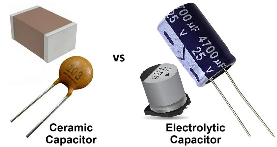
- Add Decoupling Capacitors: Place decoupling capacitors (e.g., 0.1 μF ceramic capacitors) close to IC power pins to filter out noise from the power supply. Position them within 100 mils of the pin for best results.
- Isolate Analog and Digital Sections: Keep analog and digital circuits on separate areas of the PCB to prevent digital noise from affecting sensitive analog signals.
- Shield Sensitive Traces: Use guard traces or shielding techniques around critical high-speed lines to reduce crosstalk. For instance, place a grounded trace between two adjacent high-speed signals.
By taking steps to minimize signal noise, you can ensure that your PCB prototype performs reliably even in noisy environments.
4. PCB Material Selection for Signal Integrity
The choice of PCB material has a direct impact on signal integrity, especially in high-speed PCB design. The dielectric constant (Dk) and loss tangent (Df) of the material affect signal speed and attenuation. Here's how to choose the right material for your PCB prototype:
- Understand Material Properties: Standard FR-4 material has a dielectric constant of about 4.2-4.5 and is suitable for low to medium-speed designs. For high-speed applications above 1 GHz, consider low-loss materials like Rogers 4350B with a Dk of 3.48 and lower loss tangent.
- Match Material to Application: If your prototype involves RF or microwave signals, opt for materials with stable dielectric properties over a wide frequency range. For digital high-speed designs, prioritize materials with low signal loss.
- Consider Layer Stack-Up: Work with your PCB manufacturer to design a stack-up that balances signal integrity and cost. For example, a 4-layer board with signal layers sandwiched between ground planes can improve EMI performance.
Selecting the right PCB material during the prototype stage sets the foundation for achieving optimal signal integrity and performance in your final product.
5. Best Practices for High-Speed PCB Design
High-speed PCB design introduces unique challenges to signal integrity due to faster signal transitions and tighter timing requirements. Follow these best practices to optimize your PCB prototype for high-speed applications:
- Plan for Signal Timing: Ensure that signal propagation delays are accounted for in your design. For instance, at 5 GHz, a 1-inch trace on FR-4 material introduces a delay of about 150 picoseconds, which can affect timing in critical circuits.
- Use Via Optimization: Minimize the use of vias in high-speed signal paths as they can introduce inductance and capacitance. If vias are necessary, use back-drilling to remove unused via stubs.
- Simulate Before Building: Use simulation tools to analyze signal integrity before assembling your prototype. Tools can predict issues like crosstalk or impedance mismatches, saving time and cost during testing.
- Test with Realistic Conditions: During prototype testing, simulate real-world operating conditions to identify signal integrity issues early. For example, test at maximum data rates and temperatures to stress the design.
By incorporating these high-speed PCB design practices, you can build prototypes that meet the demands of modern electronics with minimal signal integrity issues.
Conclusion: Building Better PCB Prototypes with Signal Integrity in Mind
Optimizing your PCB prototype assembly for signal integrity is a critical step in creating reliable and high-performing electronic devices. By focusing on impedance matching, trace routing techniques, minimizing signal noise, careful PCB material selection, and following high-speed PCB design best practices, you can significantly reduce the risk of signal issues and ensure your prototype performs as intended.
Signal integrity in PCB prototypes isn’t just a technical requirement—it’s a competitive advantage. A well-designed prototype saves time, reduces costs, and speeds up the journey from concept to market. Start applying these strategies in your next project, and you’ll see the difference in performance and reliability.
With the right approach and attention to detail, you can master signal integrity and build PCB prototypes that stand out in today’s demanding electronics landscape.
 ALLPCB


