ALLPCB


Definition
A sample-and-hold circuit is an electronic circuit that takes a voltage sample of the input and then holds that sample for a specified period. The time taken to acquire a sample from the input signal is called the sampling time. The duration for which the circuit holds the sampled value is called the hold time. Sampling times are typically between 1 μs and 14 μs, while hold times can be chosen as required by the application.
Circuit Diagram
The diagram below shows a sample-and-hold circuit implemented with op amps. The schematic indicates two op amps connected via a switch. When the switch is closed the circuit is in the sampling phase; when the switch is opened the circuit enters the hold phase.
Purpose
The primary motivation for using a sample-and-hold circuit arises when converting analog signals to digital. Analog signals are susceptible to noise, which degrades the reliability of analog communication. To perform digital processing or digital communication, stable samples of the analog input are required. A sample-and-hold circuit captures those analog samples and stores them on a capacitor for a defined period, producing a steady signal that can be converted by an analog-to-digital converter.
How the Sample-and-Hold Circuit Works
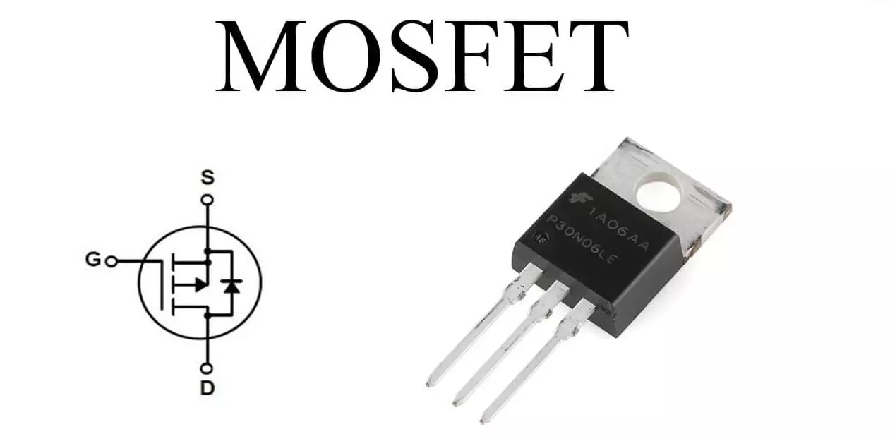
The operating principle is straightforward when examining the main components. A typical sample-and-hold circuit uses an N-channel enhancement MOSFET as the switch, a capacitor to store and hold charge, and a precision op amp to buffer the held voltage.
Input and Output Waveforms
The waveforms for sampling and holding clearly show the output voltage during the switch conduction interval and the output voltage during the hold interval when the switch is open and the op amp maintains the stored value.
Connections
The connection diagram clarifies how the input voltage and the control voltage are applied to the op amp. The capacitor used for storage should have very low leakage. Capacitors made from PTFE or polyethylene are commonly chosen when low leakage is required.
Functional Diagram
A functional block diagram helps explain the operation of the sample-and-hold circuit by showing the relationship among the input, the switching element, the storage capacitor, and the output buffer.
Performance Parameters
- Acquisition time (TAC): The time required for the capacitor to acquire the charge corresponding to the applied input voltage.
- Aperture time (TAP): The time required for the capacitor to transition from the sampling state to the hold state. Due to switch propagation delay, the capacitor may continue charging briefly after a hold command is issued; this interval is the aperture time.
- Voltage droop: The reduction in the stored voltage due to leakage of the capacitor. In practice, some voltage droop is unavoidable even with high-quality materials.
- Hold-mode settling time: After issuing a hold command, the analog input used to charge the capacitor may require some time to fully settle; this is the hold-mode settling time.
Applications
- Data distribution systems
- Sampling oscilloscopes
- Data conversion systems
- Digital voltmeters
- Analog signal processing
- Filter structures
Summary
In summary, a sample-and-hold circuit samples an analog input signal, holds the most recent sampled value for a specified period, and presents that held value at the output for subsequent processing or conversion.