If you're looking for clear guidance on BGA breakout design rules, including clearances and spacing, you've come to the right place. Ball Grid Array (BGA) components are widely used in modern electronics due to their compact size and high pin density, but designing a breakout for them can be challenging. To ensure manufacturability and reliability, you need to follow specific guidelines for pad design, routing, clearances, and spacing. In this comprehensive guide, we'll dive deep into the best practices for BGA breakout design, helping you avoid common pitfalls and achieve a robust PCB layout.
What is a BGA Breakout and Why Does It Matter?
A BGA breakout refers to the process of routing traces from the densely packed pins (or balls) of a Ball Grid Array component to other parts of the printed circuit board (PCB). Unlike traditional components with visible leads, BGA packages have solder balls arranged in a grid pattern underneath the component, making routing a complex task. A well-designed breakout ensures that signals are transmitted without interference, the board can be manufactured without errors, and the final product remains reliable over time.
Improper BGA breakout design can lead to issues like signal integrity problems, manufacturing defects, or even complete board failure. By following the right design rules, focusing on BGA breakout clearances and spacing, you can minimize these risks and create a high-quality PCB that meets both performance and production standards.
Key Challenges in BGA Breakout Design
Before diving into the specific design rules, it's important to understand the challenges associated with BGA breakouts. These components often have hundreds or even thousands of pins in a very small area, sometimes with a pitch (distance between pins) as tight as 0.4mm. This density makes routing difficult and increases the risk of short circuits or crosstalk. Additionally, BGA packages often handle high-speed signals, requiring careful attention to impedance control and signal integrity. Finally, thermal management is a concern, as BGAs can generate significant heat during operation.
With these challenges in mind, let's explore the essential BGA breakout design rules to ensure manufacturability and reliability.
Essential BGA Breakout Design Rules for Success
1. Understand BGA Pad Design and Solder Mask Rules
The foundation of a successful BGA breakout starts with the pad design. BGA pads are where the solder balls connect to the PCB, and their size and shape directly impact soldering quality during assembly. There are two common pad types for BGAs: Non-Solder Mask Defined (NSMD) and Solder Mask Defined (SMD).
- NSMD Pads: These pads are smaller than the solder mask opening, allowing the solder to flow around the pad. NSMD is preferred for most BGAs because it provides better solder joint reliability, especially for fine-pitch components with a pitch of 0.5mm or less. A typical NSMD pad diameter is about 80-90% of the solder ball diameter.
- SMD Pads: Here, the solder mask covers part of the pad, defining its size. While SMD pads can be easier to manufacture for larger pitches (above 0.8mm), they are less flexible for fine-pitch BGAs and may lead to weaker solder joints.
For manufacturability, ensure that the solder mask clearance around NSMD pads is at least 0.075mm to prevent mask overlap, which can cause soldering defects. Check with your PCB fabrication partner for their specific capabilities, as tighter tolerances may require advanced manufacturing processes.
2. Optimize BGA Breakout Clearances
BGA breakout clearances refer to the minimum distances between pads, traces, and other conductive elements to prevent electrical shorts and ensure manufacturability. Maintaining proper clearances is critical, especially for fine-pitch BGAs where space is limited.
- Pad-to-Pad Clearance: For a 0.5mm pitch BGA, maintain a minimum clearance of 0.2mm between pads to avoid solder bridging during assembly. For a 0.4mm pitch, this may need to be reduced to 0.15mm, but consult your manufacturer for their minimum requirements.
- Pad-to-Trace Clearance: Keep at least 0.1mm between pads and nearby traces to prevent unintended connections. This spacing also helps during inspection and rework processes.
- Trace-to-Trace Clearance: For high-density designs, aim for a minimum trace-to-trace clearance of 0.1mm on the same layer to avoid crosstalk and ensure reliable manufacturing.
These clearance values are general guidelines and may vary based on your PCB fabrication and assembly capabilities. Always align your design with the manufacturer's design for manufacturability (DFM) rules to avoid costly revisions.
3. Follow BGA Breakout Spacing Guidelines
BGA breakout spacing goes hand-in-hand with clearances but focuses more on the layout of traces and vias as they escape from the BGA grid. Proper spacing ensures that traces can be routed without congestion, maintaining signal integrity and manufacturability.
- Via Placement: When routing traces out of the BGA, vias are often used to transition to other layers. Place vias as close as possible to the BGA pads (ideally within 0.3mm) to minimize trace length and reduce signal degradation. Use microvias for fine-pitch BGAs to save space.
- Trace Width and Spacing: For high-speed signals, maintain a trace width of around 0.1mm to 0.15mm, with spacing of at least 0.1mm between traces on the same layer. This helps control impedance, typically targeting 50 ohms for single-ended signals or 100 ohms for differential pairs.
- Fanout Strategy: Use a "dog-bone" fanout pattern for fine-pitch BGAs, where a short trace connects the pad to a nearby via. This pattern allows for tighter spacing and efficient routing. For a 0.4mm pitch BGA, ensure the dog-bone trace length is no more than 0.5mm to minimize inductance.
Proper spacing not only aids in routing but also ensures that the PCB can be fabricated without defects like trace shorts or incomplete etching.
4. Prioritize Signal Integrity in Routing
Signal integrity is a top concern in BGA breakout design, especially for high-speed applications like DDR memory or PCIe interfaces. Poor routing can lead to crosstalk, signal delay, or electromagnetic interference (EMI).
- Minimize Trace Lengths: Keep traces as short as possible when breaking out from the BGA. For high-speed signals (above 1 GHz), aim for trace lengths under 10mm to reduce signal delay and loss.
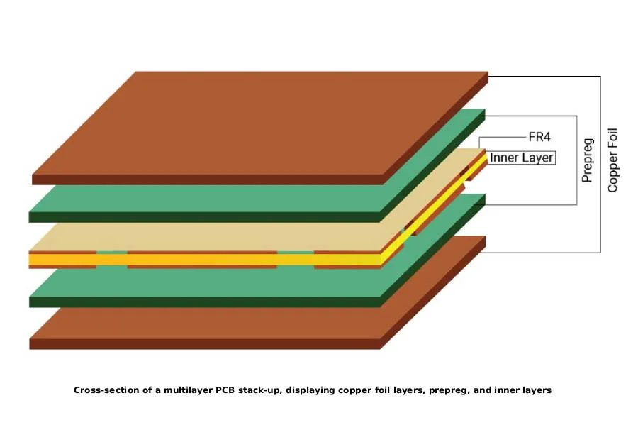
- Route on Inner Layers: Use inner layers of the PCB for critical signals to shield them from external noise. Ensure a solid ground plane is adjacent to these signal layers to provide a stable return path.
- Match Impedance: Calculate and match the trace impedance to the target value (e.g., 50 ohms for most high-speed signals). Use a stack-up with controlled dielectric thickness and material properties to achieve this.
By carefully planning your routing strategy, you can maintain signal quality even in dense BGA layouts.
5. Address Thermal Management
BGAs often house high-performance chips that generate significant heat. Without proper thermal management, this heat can degrade performance or damage the component.
- Thermal Vias: Place thermal vias under the BGA to transfer heat to a ground plane or heat sink. For a typical design, use an array of vias with a diameter of 0.3mm and a pitch of 1.2mm under the BGA's thermal pad.
- Ground Planes: Connect thermal vias to large ground planes on multiple layers to dissipate heat effectively. Ensure the ground plane is unbroken under the BGA for maximum heat transfer.
- Component Spacing: Maintain at least 2mm of spacing between the BGA and other heat-generating components to prevent thermal overlap.
Effective thermal design ensures long-term reliability, especially for BGAs in power-intensive applications.
6. Collaborate with Your Manufacturer
One of the most important BGA breakout design rules is to align your layout with your manufacturer's capabilities. Different fabricators and assemblers have varying tolerances for pad sizes, clearances, and via drilling.
- Request DFM Guidelines: Obtain the Design for Manufacturability guidelines from your PCB partner early in the design process. These will specify minimum clearances, trace widths, and other critical parameters.
- Verify Assembly Process: Confirm that the assembler can handle the BGA pitch and soldering requirements. For fine-pitch BGAs (below 0.5mm), advanced reflow soldering or X-ray inspection may be necessary.
- Prototype and Test: Build a small batch of prototypes to test the design before full-scale production. This helps identify potential issues with clearances, spacing, or soldering quality.
Close collaboration with your manufacturing partner can save time and reduce the risk of costly redesigns.
Common Mistakes to Avoid in BGA Breakout Design
Even experienced designers can make mistakes when working with BGAs. Here are some common pitfalls to watch out for:
- Ignoring Manufacturer Guidelines: Failing to follow DFM rules can lead to unmanufacturable boards. Always check the minimum tolerances for clearances and spacing.
- Overcrowding Traces: Routing too many traces in a small area without proper spacing can cause crosstalk or manufacturing defects. Use multiple layers if needed to spread out the routing.
- Neglecting Signal Integrity: Long, unmatched traces or poor grounding can degrade high-speed signals. Plan your routing carefully to avoid these issues.
- Inadequate Thermal Design: Skipping thermal vias or ground planes can lead to overheating, reducing the lifespan of the BGA component.
By being mindful of these mistakes, you can create a more reliable and manufacturable BGA breakout design.
Tools and Software for BGA Breakout Design
Modern PCB design software offers powerful features to simplify BGA breakout design. These tools often include automated fanout patterns, clearance checking, and signal integrity analysis. Look for software that supports high-density interconnect (HDI) design and provides real-time design rule checks (DRC) to catch errors early. Features like 3D visualization can also help you verify pad placement and via alignment before sending the design to fabrication.
Conclusion: Mastering BGA Breakout Design for Better PCBs
Designing a BGA breakout that ensures manufacturability and reliability requires careful attention to detail. By following the BGA breakout design rules outlined in this guide—focusing on pad design, clearances, spacing, signal integrity, and thermal management—you can create a robust PCB layout that performs well and can be produced without issues. Remember to prioritize BGA breakout clearances and spacing to avoid common manufacturing defects, and always collaborate with your fabrication and assembly partners to align with their capabilities.
Whether you're working on a fine-pitch BGA with a 0.4mm grid or a larger package, these guidelines will help you achieve a successful design. With the right approach, you can overcome the challenges of BGA breakouts and deliver high-quality, reliable electronics for any application.
 ALLPCB


