ALLPCB


In the world of printed circuit board (PCB) design, achieving optimal performance requires balancing multiple factors like signal integrity and heat dissipation. Two critical techniques that play a significant role in this balance are backdrilling PCB processes and thermal management. But how do these methods work together to enhance PCB design? In short, backdrilling improves signal integrity by reducing interference in high-speed circuits, while thermal management ensures heat dissipation to prevent component failure. This blog post dives deep into both concepts, exploring their importance, implementation, and how they create a holistic approach to modern PCB design.
Understanding Backdrilling in PCB Design
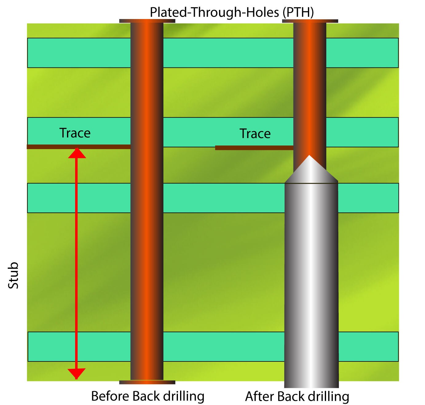
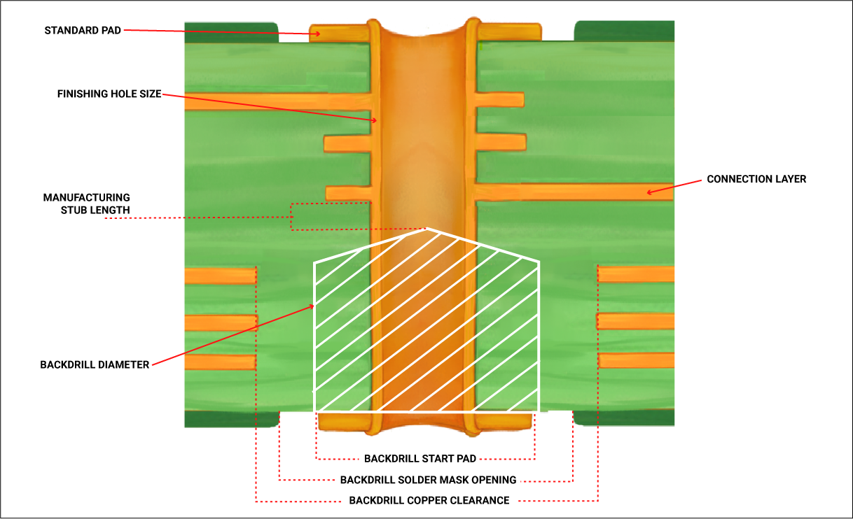
Backdrilling is a specialized manufacturing process used in PCB design to enhance signal integrity, especially in high-speed applications. When designing multilayer PCBs, plated through-holes (PTHs) are used to connect different layers. However, these holes often extend beyond the layers they need to connect, creating unused stubs. These stubs can cause signal reflections, leading to interference and degraded performance in high-speed circuits operating at frequencies above 1 GHz.
The backdrilling process involves drilling out these unused portions of the PTHs from the opposite side of the board after the initial plating. By removing the stubs, backdrilling minimizes signal reflections and reduces electromagnetic interference (EMI). For instance, in a 10-layer PCB with a signal speed of 5 Gbps, a stub length of just 0.5 mm can introduce enough reflection to disrupt data integrity. Backdrilling can reduce this stub to near zero, ensuring cleaner signals.
Benefits of Backdrilling for Signal Integrity
The primary advantage of backdrilling in PCB design is improved signal integrity. By eliminating stubs, it reduces signal distortion, which is critical for applications like telecommunications, data centers, and high-speed computing. Here are some key benefits:
- Reduced Signal Reflections: Stubs act as antennas, reflecting signals back and causing interference. Backdrilling eliminates this issue, ensuring signals travel with minimal distortion.
- Lower EMI: With cleaner signal paths, electromagnetic interference is significantly reduced, which is vital for densely packed boards.
- Support for Higher Frequencies: As data rates climb beyond 10 Gbps, backdrilling becomes essential to maintain performance without costly redesigns.
Implementing backdrilling requires precision during manufacturing, as over-drilling can damage necessary connections. Designers must also account for additional costs, as this process adds a step to production. However, for high-speed applications, the trade-off is often worth it.
The Importance of Thermal Management in PCB Design
While backdrilling focuses on signal integrity, thermal management addresses another critical challenge in PCB design: heat dissipation. As electronic devices become smaller and more powerful, components generate more heat in confined spaces. Without proper heat dissipation, temperatures can rise beyond safe limits, leading to reduced performance, shortened component lifespans, or even complete failure.
For example, a power-intensive IC operating at 3.3V with a current draw of 2A can generate significant heat, raising local temperatures to over 100°C if not managed properly. Effective thermal management ensures this heat is dissipated, maintaining safe operating conditions around 60-85°C for most components.
Key Techniques for Heat Dissipation in PCBs
There are several proven methods for managing heat in PCB design. Each technique can be tailored to specific applications, depending on the power density and space constraints. Below are some widely used strategies:
- Thermal Vias: These are small holes filled or plated with conductive material, typically copper, that transfer heat from hot components to other layers or a heat sink. Arrays of thermal vias under a high-power component can reduce temperatures by 10-15°C.
- Heat Sinks: Attached directly to high-heat components, heat sinks absorb and dissipate heat into the surrounding air. They are often paired with thermal vias for maximum effect.
- Copper Planes: Large areas of copper on the PCB act as heat spreaders, distributing heat evenly across the board. A solid copper plane can lower peak temperatures by up to 20% compared to a board without one.
- Advanced Materials: Using substrates with higher thermal conductivity, such as metal-core PCBs, can improve heat dissipation significantly. These materials are ideal for LED lighting or power electronics.
Proper thermal management not only protects components but also enhances overall reliability. Overheating can cause solder joints to crack or components to degrade, leading to costly failures in the field.
Integrating Backdrilling and Thermal Management: A Holistic Approach
While backdrilling PCB techniques and thermal management address different challenges, they are not mutually exclusive. In fact, combining these approaches creates a holistic PCB design strategy that optimizes both signal integrity and heat dissipation. Modern high-performance electronics, such as 5G infrastructure or AI hardware, demand this integrated approach to meet stringent performance and reliability standards.
For instance, in a multilayer PCB for a high-speed server, backdrilling ensures clean signal transmission at data rates of 25 Gbps or higher. At the same time, the dense packing of components and high power draw necessitate robust thermal management to keep temperatures below 80°C. Designers must carefully plan the placement of thermal vias and copper planes to avoid interfering with backdrilled holes, ensuring both techniques work in harmony.
Challenges in Combining Backdrilling and Thermal Management
Integrating these two techniques is not without challenges. Backdrilling removes material from the board, which can affect thermal conductivity if not planned properly. For example, excessive backdrilling near a high-heat area might reduce the effectiveness of thermal vias or copper planes. Designers must use simulation tools to model both signal and thermal behavior before finalizing the layout.
Additionally, manufacturing constraints can complicate the process. Backdrilling requires precise control to avoid damaging nearby structures, while adding thermal vias increases the complexity of drilling and plating. Balancing these factors often requires close collaboration between design and manufacturing teams.
Best Practices for a Balanced PCB Design
To successfully combine backdrilling PCB techniques with thermal management, consider the following best practices:
- Use Simulation Software: Tools for signal integrity and thermal analysis can predict potential issues before manufacturing. For example, simulating a design with a 50-ohm impedance requirement can confirm that backdrilling won’t disrupt critical paths.
- Optimize Via Placement: Place thermal vias strategically to maximize heat transfer without interfering with backdrilled holes. A grid pattern under hot components often works best.
- Plan Layer Stackup: Design the layer stackup to separate high-speed signal layers from power-heavy layers, minimizing interference while supporting thermal dissipation through dedicated copper planes.
- Select Appropriate Materials: Choose board materials that balance electrical and thermal properties. For high-speed designs, low-loss dielectrics are crucial, while high-thermal-conductivity substrates aid in heat dissipation.
By following these practices, designers can create PCBs that excel in both signal integrity and heat dissipation, ensuring reliable performance in demanding applications.
Real-World Applications of Backdrilling and Thermal Management
The integration of backdrilling and thermal management is already making a difference in various industries. In telecommunications, 5G base stations rely on high-speed signals and generate significant heat due to dense component layouts. Backdrilling ensures data integrity at frequencies up to 28 GHz, while thermal vias and heat sinks keep critical components cool under heavy loads.
In automotive electronics, advanced driver-assistance systems (ADAS) require robust PCB design to handle high-speed data processing and power management. Backdrilling reduces signal noise in radar and camera modules, while copper planes and heat sinks dissipate heat from power-intensive processors, ensuring reliability in harsh environments.
Future Trends in PCB Design: Evolving Techniques
As technology advances, the demands on PCB design will continue to grow. Data rates are expected to exceed 50 Gbps in the near future, making backdrilling even more critical for maintaining signal integrity. At the same time, the push for miniaturization will increase heat density, requiring innovative thermal management solutions like embedded heat pipes or advanced composite materials.
Designers will also benefit from improved simulation tools that integrate signal and thermal analysis into a single platform. These tools will allow for more accurate predictions and faster iterations, reducing time-to-market for complex designs.
Conclusion: Building Better PCBs with a Holistic Approach
In summary, combining backdrilling PCB techniques with effective thermal management offers a powerful solution for modern PCB design. Backdrilling enhances signal integrity by eliminating unwanted stubs, while heat dissipation strategies like thermal vias and copper planes ensure components operate within safe temperature ranges. By integrating these methods, designers can create PCBs that meet the high-performance demands of today’s electronics, from 5G networks to automotive systems.
At ALLPCB, we understand the importance of balancing these factors to deliver reliable, high-quality boards. Whether you’re tackling high-speed signals or managing intense heat loads, adopting a holistic approach to PCB design is the key to success. With careful planning and the right techniques, your next project can achieve unparalleled performance and durability.