My Message
 Suggestions


1. Normally, all components should be placed on the same side of the boards. Only when the top layer is too dense can some devices with limited height and low heat generation, such as patch resistance, patch capacitance and patch IC, be placed at the bottom layer.
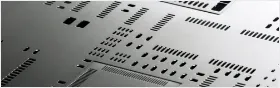
2. In order to make sure the electrical property, the element shall be located on the gridlines and in alignment, to keep it natty and artistic. The elements should be compact in arrangement, and they should be uniformly distributed and spaced on the whole layout.
3. The minimum spacing between the shapes of different components on the circuit board should be more than 1MM.
4. When the circuit board is larger than 200MM x 150MM, the mechanical strength of the circuit board should be considered.
5. On many PCB which have high voltage and low voltage circuit, at the same time of the components of high voltage circuit with low voltage part to open space, distance between related to bear pressure, is often the case in the 2000 kv distance on the PCB to 2 mm, on top of this ratio is also increased. For example, if you want to bear the pressure test of 3000 v, the distance between the high and low voltage lines should be above 3.5 mm, in many cases to avoid creepage, also on the PCB board slot between high and low pressure.
6. The arrangement of printed wires should be as short as possible, especially in high frequency circuits. The bending of the printed conductor should be rounded, and the right Angle or sharp Angle will affect the electrical performance under high frequency circuit and high density of wiring. When two panels are wired, the wires on both sides should be perpendicular, oblique or curved to each other to avoid being parallel to each other, so as to reduce parasitic coupling. The printed conductors used for the input and output of the circuit should avoid adjacent parallel lines as far as possible, so as to avoid the occurrence of feedback. It is advisable to add grounding wires between these conductors.
In the layout design of PCB, the elements of the circuit board should be analyzed, and the layout design should be carried out according to the functions. When all components of the circuit are laid out, the following principles should be followed:
1. Arrange the position of each functional circuit unit according to the circuit flow, make the layout convenient for signal flow, and keep the signal as consistent as possible.
2. Centered around the nuclear elements of each functional cell, the layout is distributed about it. Element shall be equably, collectively and tightly placed on the boards to decrease and shorten the wires and links among elements.