

● Top- and Bottom-side Masks
● Epoxy Liquid Solder Masks
● Liquid Photoimageable Solder Masks
● Dry Film Photoimageable Solder Masks
Instant Quote
Full feature prototype PCB custom service at low cost.
Flexible PCB
Customized FPC service with high standards
Rigid-Flex PCB
High precision rigid-flex PCB customized service
PCB Assembly Quote
Leading assembly factory with Siemens production line
SMD-Stencil
Laser cutting high precision stencil service
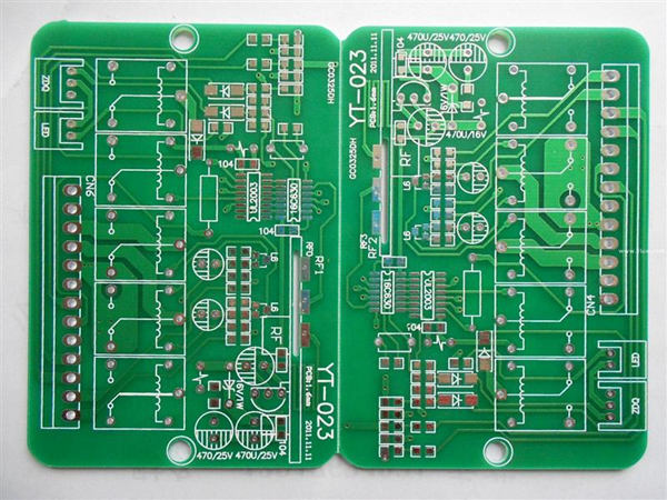
Solder mask, also known as solder resist is a strong, permanent layer that protects copper traces and the interfaces between them on printed circuit boards (PCBs). The main function of a solder mask is to prevent conductive solder bridging between different electronic components and causing short circuits. There are many types of PCB soldermask, such as Epoxy Liquid, Liquid Photoimageable, Dry Film Photoimageable, Top- and Bottom-side Masks.

Soldermask Types
Top- and Bottom-side Masks
A topside solder mask allows the electronic engineer to identify the openings in the green solder mask layer already added to the PCB by one of the epoxy, ink or film techniques. Component pins can then be soldered onto the board using those identified places. The pattern of conductive traces on the topside of the circuit board is called top traces and the bottom-side mask specifies openings on the lower surface.
Epoxy Liquid
Silkscreened onto the PCB pattern, epoxy liquid is the lowest cost type of solder mask. Epoxy is a thermosetting polymer that has many applications. Silkscreening is a printing technique that uses a woven mesh to support ink-blocking stencils or patterns. The mesh creates open areas for ink transfer. Silk is often used in art but synthetic fibers are more common for electronic applications. The final finishing process involves thermal curing.
Liquid photoimageable solder mask is delivered as an ink formulation. The ink can be silkscreened or sprayed onto the PCB, then exposed to the pattern and developed. One type of process commonly used with liquid ink formulations is hot air surface leveling (HASL). It requires a clean environment, free of particles and contaminants. After the UV light exposure stage, the mask is removed using high-pressure water sprays called developers. Circuit board finishing requires thermal curing and organic coating.
Dry film photoimageable solder mask is applied using vacuum lamination, then exposed and developed. After developing, openings are created in the pattern and parts can be soldered to the copper pads. Copper is layered onto the board inside the holes and on the trace areas using electrochemical processing. Tin is applied to protect the copper circuitry. The dry film is then removed and the exposed copper etched. Finishing also involves thermal curing.


Terms of Service | Privacy Policy | Refund Policy | Sitemap
© ALLPCB.com, All Rights Reserved


