 ALLPCB
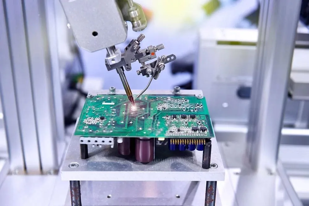
Mastering PCB Drilling: A Comprehensive Guide to Techniques, Equipment, and Best Practices
Master PCB drilling with our guide on CNC, laser, and automated techniques. Explore equipment, methods, and best practices for engineers.



Master PCB drilling with our guide on CNC, laser, and automated techniques. Explore equipment, methods, and best practices for engineers.

Explore green soldering with lead-free solder PCB options, recyclable solder, and RoHS compliant materials for sustainable PCB manufacturing.

Learn about PCB edge plating: applications like EMI shielding, grounding, and thermal management, plus design guidelines for engineers.
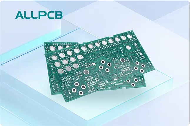
Explore conformal coating for high-frequency PCBs to minimize signal loss and ensure performance. Learn about dielectric constant and RF circuits.

Discover microvia testing for reliable HDI PCBs. Learn failure modes, testing methods, and best practices to optimize your PCB designs for engineers.

Explore how PCB plating impacts signal integrity, covering signal loss, RF circuits, impedance matching, and EMI shielding for engineers.

Compare ENIG vs. Electroplating for PCB gold fingers. Explore benefits, drawbacks, cost, and performance to choose the best plating method.

Explore advanced PCB recycling technologies like pyrometallurgy, hydrometallurgy, and electrochemical methods for sustainable material separation.

Discover bio-based flexible PCBs, the future of sustainable electronics. Explore eco-friendly materials, benefits, and innovations for greener tech.

Explore IPC-A-600 standards for solder mask coverage and registration. Learn tips for PCB quality and inspection with ALLPCB expertise.

Discover practical solutions for PCB surface finish defects like HASL uneven coating, ENIG black pad, and OSP oxidation in this ALLPCB guide.

Optimize PCB performance with the right solder mask thickness. Learn about insulation, durability, impedance control, and more in this guide.

PTFE PCB dielectric constant from 2.1 to 2.6 and low loss tangent of 0.0002 to 0.002 deliver top signal performance in high-frequency designs. This guide details electrical properties, measurement methods per IPC-TM-650, influencing factors, best practices, and troubleshooting for reliable RF boards.

Learn how to validate PCB manufacturing processes for ISO 13485 compliance. Ensure quality and safety in medical device production with our detailed guide.

Explore multi-layer PCB stackup design for high density. Learn impedance control, signal integrity, and cost-effective tips in this deep dive.
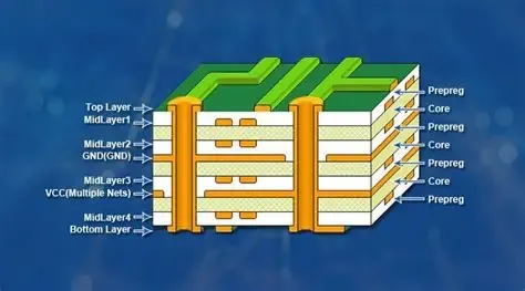
Learn PCB design review steps and DFM process flow in this step-by-step guide. Master how to conduct an effective DFM review for reliable PCB manufacturing.
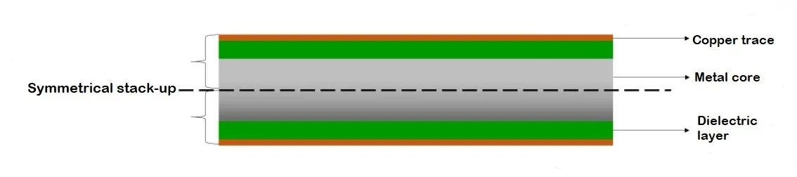
Ground plane design signal integrity and DFM strategies for EMI reduction PCB using optimized signal return paths in high-speed designs.

Explore AOI vs. AXI PCB inspection methods. Learn their differences, benefits, and best uses for your project with ALLPCB's expert guide.
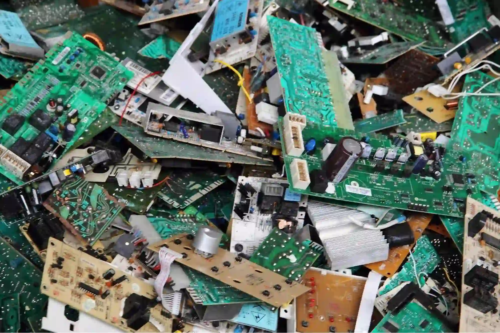
Explore the environmental impact of improper PCB disposal and why recycling matters to combat pollution and protect ecosystems.

Discover practical solutions for FR-4 PCB manufacturing defects with this troubleshooting guide. Learn to identify and repair issues effectively.