 ALLPCB

PCB lamination process and impact on manufacturing time
Explore the PCB lamination process and its impact on manufacturing time. Learn about materials, temperature, and steps for multilayer PCBs.



Explore the PCB lamination process and its impact on manufacturing time. Learn about materials, temperature, and steps for multilayer PCBs.

Explore common PCB plating defects, their causes, and prevention tips. Learn troubleshooting and quality control for reliable manufacturing.

Learn to troubleshoot PCB lamination defects like delamination, voids, and warpage with practical tips for engineers in this detailed guide.

Learn to prevent PCB corrosion with tips on electrochemical migration (ECM), CAF, cleaning methods, and conformal coating in this ALLPCB guide.

Static vs. Dynamic Burn-In: Learn the advantages, applications, and comparison of testing methods to choose the best for your PCB assembly.

Explore the hidden costs of PCB defects and master quality control in mass production with AOI, X-ray inspection, and defect prevention tips.

PTFE PCB dielectric constant from 2.1 to 2.6 and low loss tangent of 0.0002 to 0.002 deliver top signal performance in high-frequency designs. This guide details electrical properties, measurement methods per IPC-TM-650, influencing factors, best practices, and troubleshooting for reliable RF boards.

Learn how PCB lamination temperature control optimizes resin flow and curing for high-quality boards. Explore FR-4 parameters and best practices.
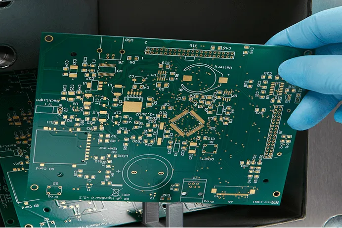
Master PCB plasma etching with our guide for engineers. Learn processes, parameters, RF & ICP etching, and equipment for precision results.
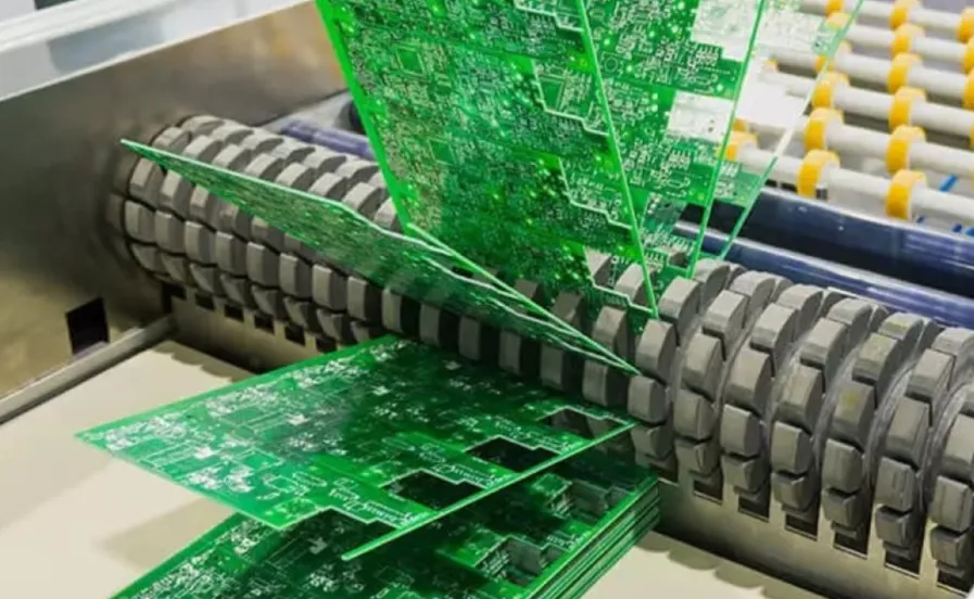
With the advent of Industry 4.0, mass production of PCBs not only needs to meet the demand in terms of quantity, but also needs to integrate the new trends of intelligence, automation and informationization.