 ALLPCB

PCB Direct Imaging: The Future of Multi-Layer PCB Alignment
Explore PCB Direct Imaging and LDI for multi-layer PCB alignment. Learn how it ensures precision and shapes the future of manufacturing.



Explore PCB Direct Imaging and LDI for multi-layer PCB alignment. Learn how it ensures precision and shapes the future of manufacturing.

Explore our guide on PCB rework stations for SMT components. Learn about SMT and SMD rework tools, tips, and best practices for precision work.

Explore X-ray PCB inspection for detecting internal defects. Learn the non-destructive testing process and ensure quality with this deep dive.

Explore PCB lamination pressure's role in quality and reliability. Learn pressure control, uniform application, and HDI defect prevention.

Learn best practices for maintaining PCB plating quality with tips on control, maintenance, inspection, and testing for reliable results.

Learn how PCB panelization boosts efficiency and cuts costs in manufacturing. Explore methods, benefits, and tips for engineers to optimize PCB production.

Optimize PCB assembly with stencil design for panelization. Learn aperture size, thickness, step stencil, and solder defect prevention tips.

Learn PCB impedance testing with this guide on methods, signal integrity, and controlled impedance design for high-performance PCB projects.
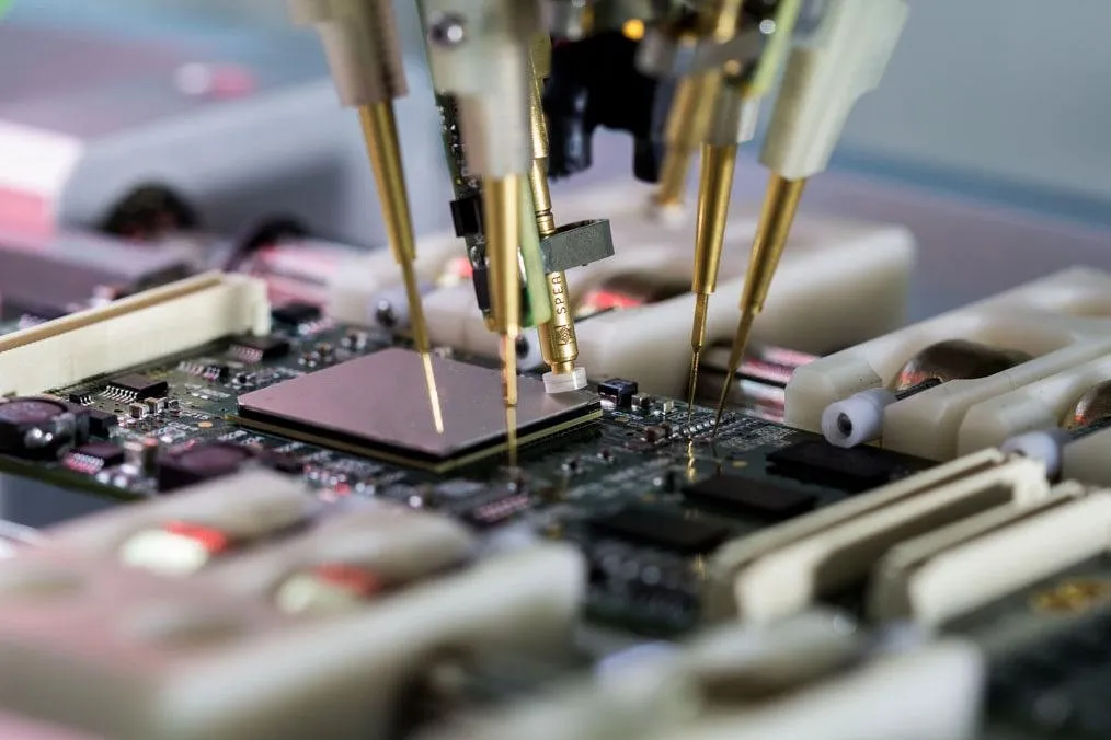
Explore if flying probe testing suits your small batch PCB production. Learn its benefits, costs, and applications for low-volume manufacturing.

Discover Flying Probe PCB Testing, the agile solution for prototypes and low-volume production. Learn its benefits, costs, and services.