 ALLPCB
Navigating Design Rules: A Practical Guide to Blind and Buried Via Spacing and Clearance
Learn PCB via spacing, blind & buried via clearance rules in this practical guide to enhance your PCB design with actionable tips from ALLPCB.



Learn PCB via spacing, blind & buried via clearance rules in this practical guide to enhance your PCB design with actionable tips from ALLPCB.
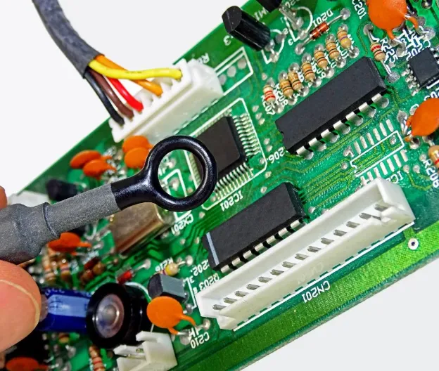
Troubleshoot PCB plasma etching issues like uneven etching, over-etching, and residue. Learn solutions for common defects in PCB fabrication.
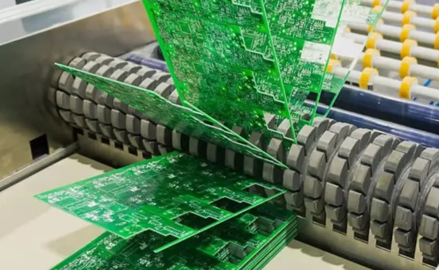
With the advent of Industry 4.0, mass production of PCBs not only needs to meet the demand in terms of quantity, but also needs to integrate the new trends of intelligence, automation and informationization.

Learn impedance control in PCB routing with best practices on trace spacing, via placement, and signal return paths for optimal design.

Explore beyond FR-4 with high-temperature PCB laminates and low CTE materials to prevent delamination in extreme aerospace and automotive settings.

Explore Flex PCB connectors and IPC-6013 connection requirements for reliable flexible circuit termination and connector selection.

Discover when to use ENIG finish on PCBs for your electronics projects. Learn ENIG benefits for hobbyists and how to improve PCB quality.

Rogers RO4350B datasheet reveals properties like Dk 3.48 and Df 0.0037 for high frequency PCB applications. Covers impedance control, signal loss reduction, RF uses in 5G and radar, plus fabrication best practices for electrical engineers seeking reliable performance.

Explore why PCB impedance testing is vital for signal integrity. Learn about TDR measurement, differential testing, and controlled impedance manufacturing.
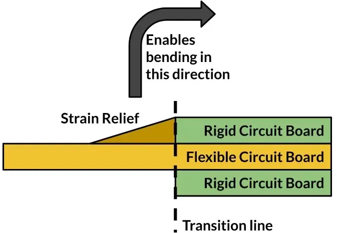
Explore rigid-flex PCB manufacturing with ALLPCB. Learn bend radius calculation, dynamic flex design, and IPC-2223 standards for optimal performance.