 ALLPCB

The Role of Ground Planes in Reducing Electromagnetic Interference
Learn how PCB ground planes reduce EMI, enhance signal integrity, and ensure EMC compliance with practical design tips for engineers.



Learn how PCB ground planes reduce EMI, enhance signal integrity, and ensure EMC compliance with practical design tips for engineers.
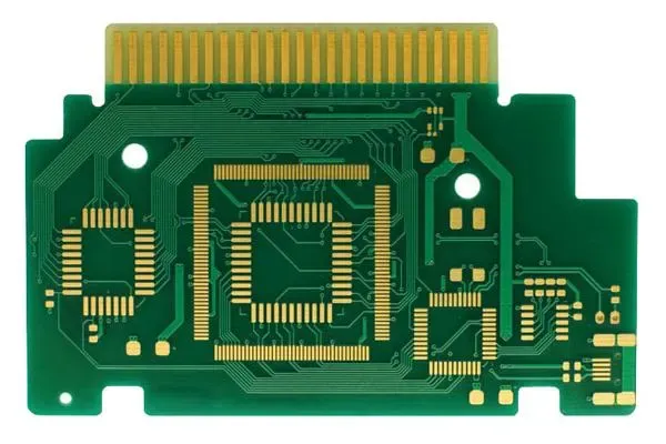
Learn the step-by-step electrolytic gold plating process for PCB gold fingers, from nickel plating to controlling thickness for durability.
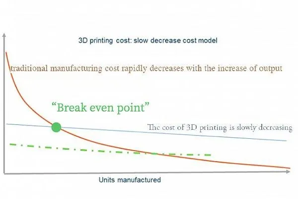
Explore 3D printing PCBs for prototyping and custom manufacturing. Learn about materials, costs, and additive processes revolutionizing design.
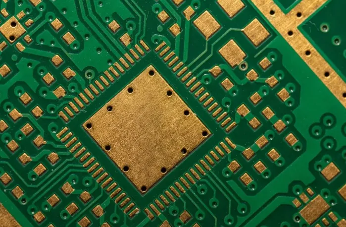
Explore PCB gold finger alternatives like ENIG, immersion silver, and palladium-nickel. Compare costs and performance for cost-effective finishes.
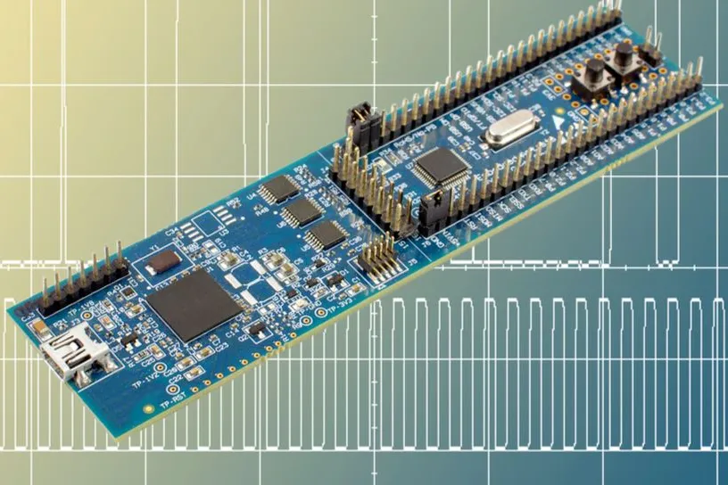
Explore the PCB prototype manufacturing process with our step-by-step guide. Learn design, Gerber files, fabrication, and assembly tips at ALLPCB.
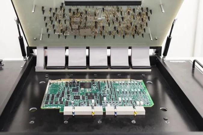
Discover why electronic component burn-in testing is vital for reliability in manufacturing. Learn methods to prevent failures with ALLPCB.
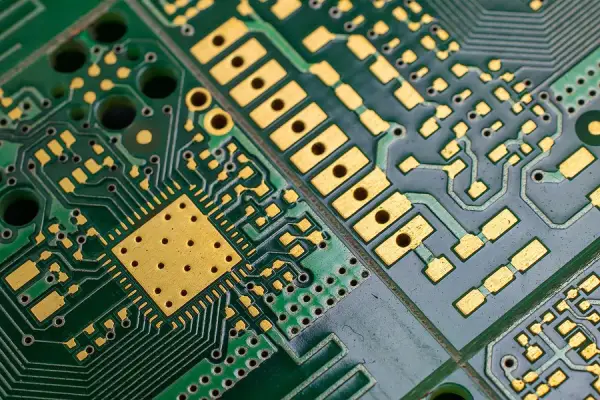
Explore the differences between ENIG vs Gold Plating for PCB boards. Learn their benefits, drawbacks, and ideal applications in this guide.
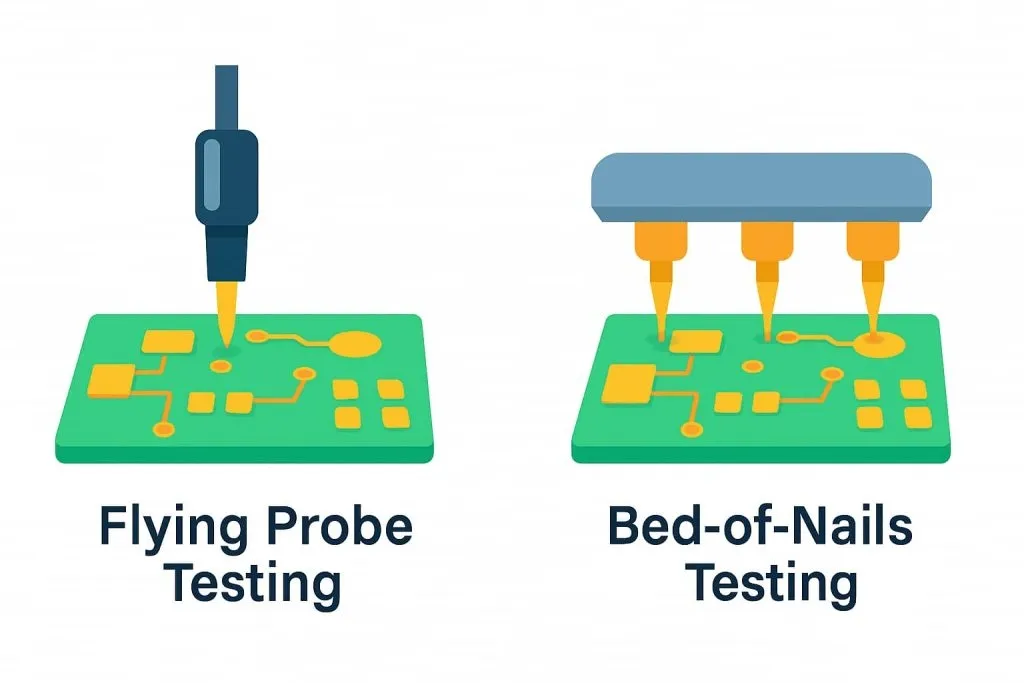
Explore flying probe vs. bed-of-nails testing in our PCB testing methods comparison. Learn advantages and choose the right strategy for your project.
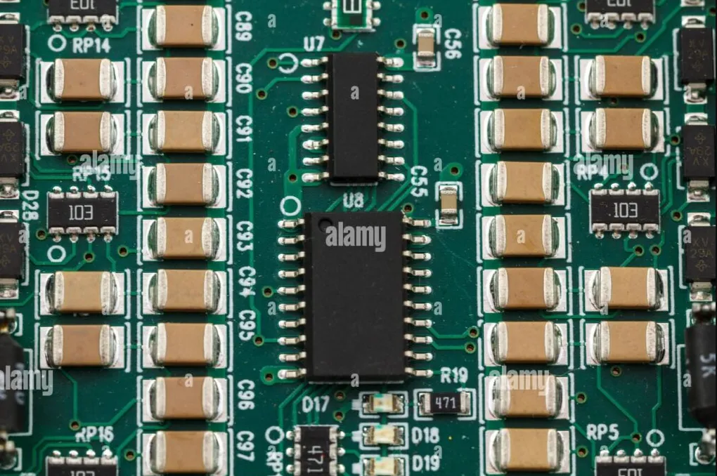
Decode PCB component codes with this guide for hobbyists. Learn to understand electronics parts and build transparent PCB projects with ease.

Learn best practices for BGA rework on high-density PCBs, with tips on replacement, soldering techniques, and advanced component repair.