 ALLPCB
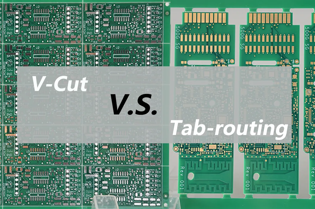
V-Scoring vs. Routing: Choosing the Right PCB Depaneling Method
Explore V-scoring vs. routing for PCB depaneling. Compare cost, edge quality, and design flexibility to choose the best method for your project.



Explore V-scoring vs. routing for PCB depaneling. Compare cost, edge quality, and design flexibility to choose the best method for your project.

ENEPIG thickness IPC 4556 covers nickel 3 to 6 micrometers, palladium 0.05 to 0.15 micrometers, gold 0.03 to 0.07 micrometers. Details layer roles, measurement methods, best practices, troubleshooting defects, and FAQs for electric engineers following PCB plating standards.

Learn high-speed digital PCB design for beginners with this guide on materials, simulation, and open-source software from ALLPCB.
Explore DBC vs FR4 in PCB thermal conductivity comparison. Learn ceramic PCB benefits and high-temperature materials for better heat management.
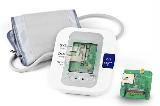
Learn HDI PCB basics with this beginner's guide. Understand what HDI PCB is, its features, applications, and design tips for modern electronics.

Explore IMS PCBs for superior thermal performance. Learn about thermal conductivity, heat dissipation, and design tips with ALLPCB.

Explore OSP vs HASL and ENIG in this PCB finish comparison. Find the best surface finish choice for your DIY electronics project with our guide.
Learn green solder mask troubleshooting with this guide for PCB repair, rework, visual inspection, and fixing solder mask defects.
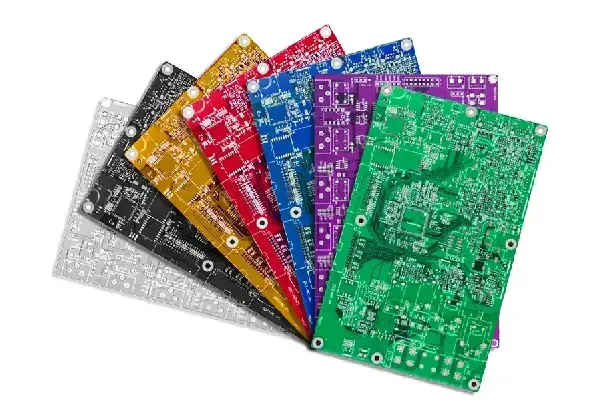
Explore how solder mask color affects PCB manufacturing cost and lead time. Learn about green solder mask price, custom colors, and fabrication costs.
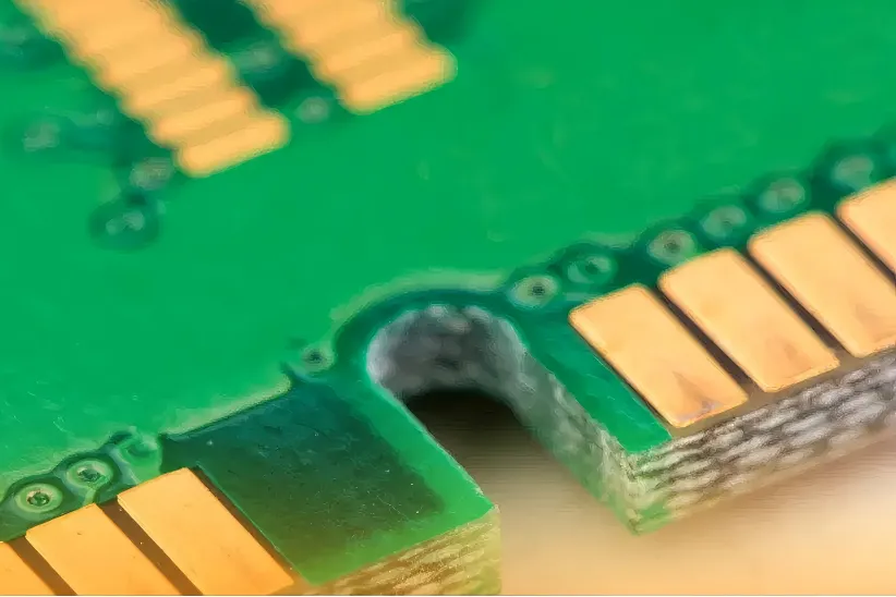
Discover best practices for gold plating in PCB manufacturing, with tips to avoid defects, troubleshoot issues, and improve quality.

Learn to optimize air quality monitoring PCB design for sensor accuracy with tips on layout, noise reduction, and BME680, PMS5003, MQ135 sensors.

Explore the pros and cons of immersion tin for PCB design, covering solderability, surface flatness, tin whiskers, and storage challenges.

Explore 7 essential aerospace PCB design rules for unwavering reliability. Learn thermal management, routing tips, and IPC-A-610 Class 3 standards.
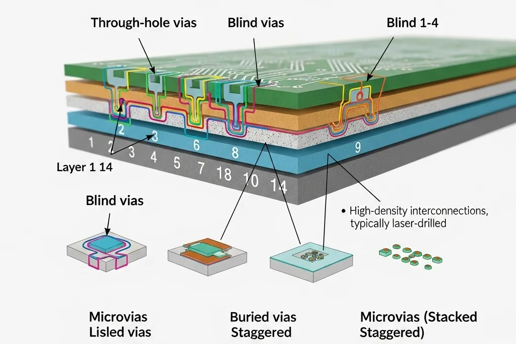
Ultimate guide to via design in 14-layer PCBs, covering via types, via-in-pad, blind/buried vias, high-density vias, and microvia design tips.

Learn multi-board panelization with edge rails in this detailed guide on design, manufacturability, and production workflow by ALLPCB.
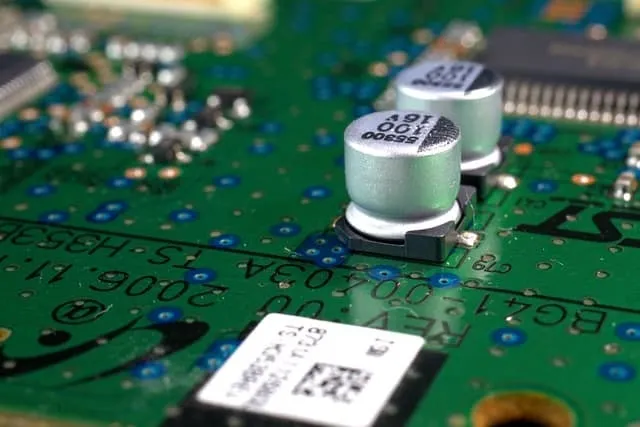
Explore dry film solder mask application techniques in PCB manufacturing. Compare vacuum lamination and hot roll lamination for precise circuit board protection.
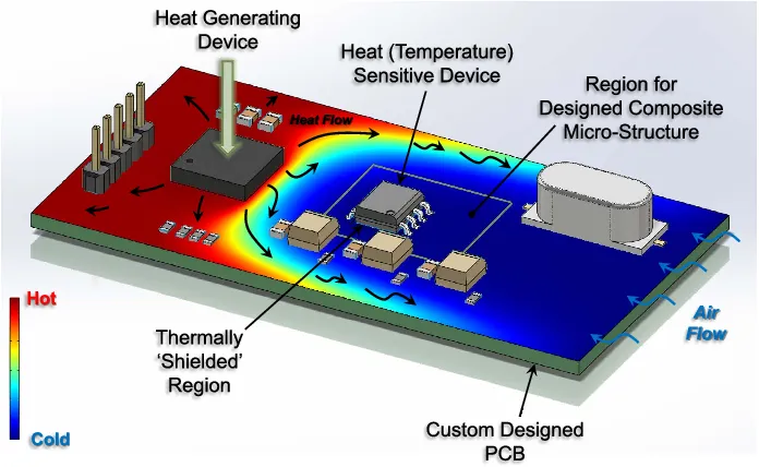
Explore thermal considerations in PCB design. Learn PCB thermal management, heat dissipation, cooling techniques, and high-power design tips.
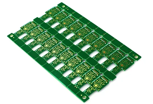
Explore PCB depanelization methods: mouse bites vs. V-scoring. Learn advantages, costs, and best uses for your project with ALLPCB.
Learn how to choose the right prepreg thickness for high-speed PCB design. Optimize signal integrity and reduce signal loss with expert tips.
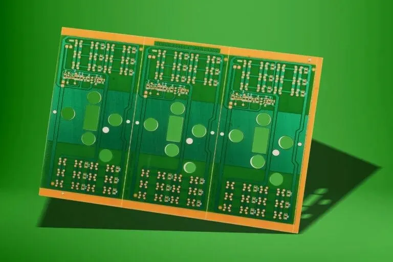
Learn the CEM-1 PCB manufacturing process with this step-by-step guide for beginners, covering etching, drilling, and single-sided fabrication.