 ALLPCB

FR 4 vs. Rogers PCB: When to Splurge for Performance
FR-4 vs. Rogers PCB: Compare cost, performance, and limitations for high-speed designs. Learn when to splurge for top performance with ALLPCB.



FR-4 vs. Rogers PCB: Compare cost, performance, and limitations for high-speed designs. Learn when to splurge for top performance with ALLPCB.

Learn wearable PCB design with KiCad in this tutorial. Master open-source PCB software for compact, efficient wearable electronics projects.

Explore standard PCB thickness options beyond 1.6mm. Learn about PCB thickness applications, comparisons, and ideal uses for your projects.

Learn pad-to-pad spacing for PCB design with DFM guidelines, solder bridging prevention, and IPC standards in this practical guide.

Learn about minimum trace spacing for PCB layers, including inner and outer layers, to ensure safety and signal integrity in your designs.

Explore dielectric strength's impact on PCB material properties, FR4, dielectric constant, and signal propagation speed in PCB design.
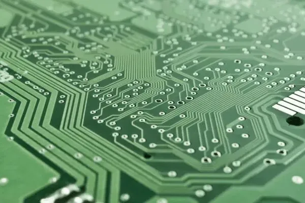
Discover the ultimate guide to minimum line width for high-current PCBs. Learn trace width, thermal management, and safety tips for reliable designs.

Explore minimum drill sizes for NPTH in PCB design, with applications and guidelines for mounting holes and mechanical PCB holes at ALLPCB.

Master PCB panelization with our guide on mouse bites. Learn design rules, hole size, spacing, and compare mouse bites vs V-score for efficiency.

Explore ENIG vs Hard Gold Plating for PCBs. Compare advantages, disadvantages, and best uses in this detailed surface finish guide by ALLPCB.
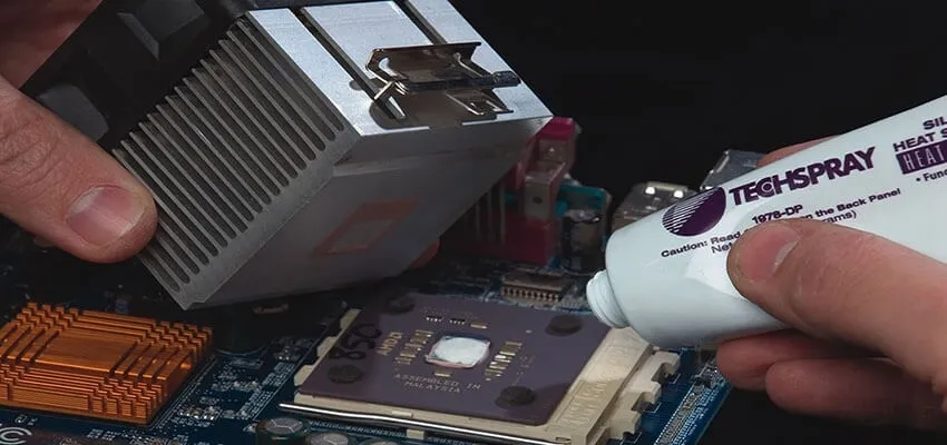
Explore heat sink attachment methods for PCBs, including thermal tape, adhesive, Z-clips, and push pins, to optimize thermal management.

Creepage distance pollution degree sets PCB surface spacing rules based on contamination levels and IEC 60664 standards. This article explains pollution degrees, industrial environment challenges, design practices like coatings, and troubleshooting for safe, reliable boards.

Explore thermal management strategies for spacecraft electronics PCBs, including thermal vias, heat dissipation, and PCB design tips for space.

Explore stacked vs. staggered blind and buried vias in HDI PCB design. Learn via reliability, routing tips, and key design rules for optimal results.

Learn how line width in mils affects PCB trace impedance. Essential tips for impedance control and routing in high-speed PCB design.
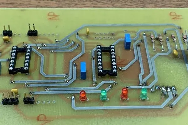
Learn the PCB etching process with our step-by-step guide to copper cladding removal using ferric chloride for hobbyists. Create homemade PCBs!

Learn to master hard gold plating thickness for PCBs, balancing cost, performance, and reliability with expert tips and standards.
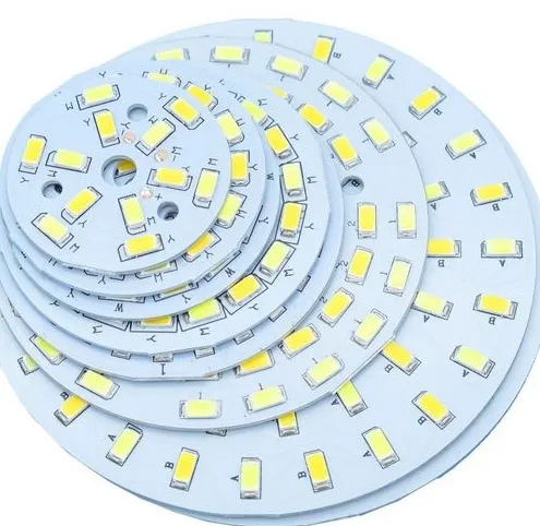
Explore high-density LED PCB design for brighter, efficient lighting. Learn thermal via optimization, micro-via techniques, and high-current guidelines.

Explore PCB design for panelization with key rules on panel size, clearance, and borders. Optimize your PCB layout for efficient manufacturing.
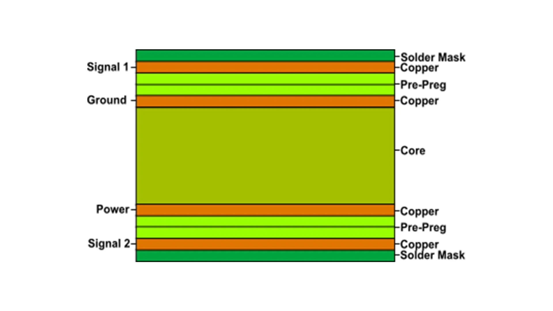
Explore signal layers in PCB design with this comprehensive guide. Learn basics, types, stackups, and tips for optimal signal integrity.