 ALLPCB

Miniaturization Methods: Designing Compact PCBs for Smart City Sensors
Explore miniaturization methods for compact PCBs in smart city sensors, focusing on HDI, microvia, and space-saving designs for efficiency.



Explore miniaturization methods for compact PCBs in smart city sensors, focusing on HDI, microvia, and space-saving designs for efficiency.

Find the best PCB design software for thick boards with our detailed guide. Learn key features, compare tools, and get practical tips to choose the right CAD software for complex multilayer PCB projects.
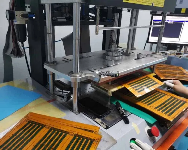
Flex PCB impedance control depends on precise PCB thickness in flexible circuits. This article covers dielectric effects, design factors, best practices, manufacturing challenges, and standards to ensure signal integrity and reliable high-speed performance for engineers.

Explore advanced mechanical drilling techniques for blind and buried vias in multilayer PCB design. Optimize space and signal integrity with ALLPCB.

Explore how controlled depth drilling enhances signal integrity in advanced PCBs, reducing signal loss and via stub effects in high-frequency designs.

Enhance rigid flex PCB reliability with stiffeners. Learn how these flex PCB support structures prevent warpage and improve solder joint integrity during rigid flex PCB assembly, ensuring robust designs.

Explore the role of vias in outer layer PCB design, focusing on PCB vias, via placement, signal integrity, blind vias, and buried vias.

Learn how panelization streamlines SMT rework and PCB repair with strategies for efficient component replacement and rework station setup.

Explore stacked via reliability in PCBs, covering testing, thermal cycling, via cracking, material selection, and durability strategies.

Learn when to use heavy copper PCBs for high current capacity and thermal management. This guide covers key applications and design rules for thick copper layers.

Learn to design high-efficiency renewable energy PCBs with tips on layout, thermal management, and low power design in this comprehensive guide.

Explore via types in mobile phone PCBs like through-hole, blind, buried, microvia, and via-in-pad, and how they enhance connectivity and design.

Learn why impedance control matters in PCBs for better performance and reliability. Explore benefits, advantages, and consequences of poor control.

Learn digital signage PCB design with this beginner's step-by-step guide. Master display PCBs, layouts, and software for advertising screens.

Explore techniques for compact PCB designs in edge computing, including HDI, component optimization, and via selection for small spaces.

Learn how outer layer copper thickness affects trace impedance in high-speed digital PCB designs for optimal signal integrity and performance.

Explore why black pads are bad for PWBs, their effects, defects, and key design considerations to avoid costly failures in electronics.

Explore the future of PCB signal layers with emerging trends like 3D PCBs, embedded components, and advanced materials for better performance.

Explore how copper weight impacts trace-to-pad spacing in PCB design, affecting trace width, current capacity, voltage drop, and thermal management.

Follow this beginner guide to calculate PCB aspect ratio with the simple formula. Learn about board thickness, via hole diameter, step by step process, real examples, and tips to ensure reliable manufacturing for your electronic hobby projects. Avoid common plating defects and build better boards.