 ALLPCB
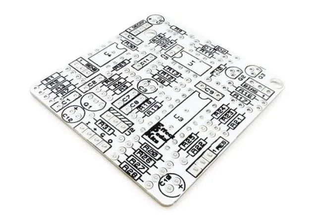
DIY Guide: Applying Silkscreen to the Bottom Layer of Your PCBs at Home
Learn how to apply silkscreen to the bottom layer of your PCB at home with this DIY guide. Master toner transfer for hobbyist PCB projects!



Learn how to apply silkscreen to the bottom layer of your PCB at home with this DIY guide. Master toner transfer for hobbyist PCB projects!
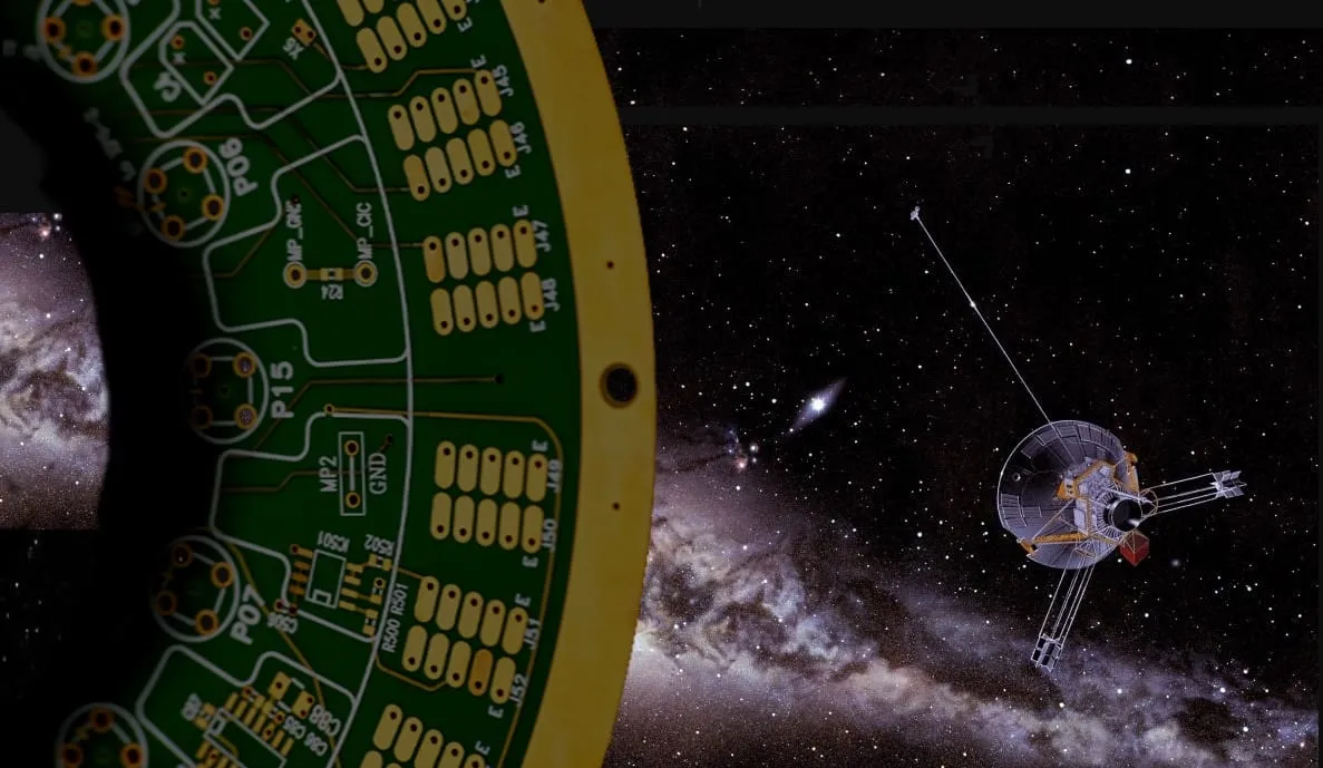
Explore our guide on choosing space-grade PCB materials for space probes, covering substrates, outgassing, and high-frequency options.

Explore signal integrity issues in mobile phone PCB layout, their causes like signal reflection, and solutions including impedance matching and crosstalk reduction.
Explore soft gold plating vs other finishes for connectors. Compare signal integrity, low-voltage performance, and durability in this guide.

Explore Immersion Tin vs OSP for SMT assembly. Learn their impact on solder paste, reflow, and joint quality to choose the best surface finish.

Explore 8-layer PCB design for aerospace, focusing on reliability, vibration, thermal, and radiation standards for mission-critical systems.

Explore the pros and cons of copper foil thickness in PCBs, including benefits of thicker copper and drawbacks of thinner copper. Read now!

Explore high-precision current sensing in EV battery management PCBs, covering design techniques, challenges, and solutions for accuracy.

Explore the benefits of Laser Direct Imaging (LDI) in high-layer-count PCB manufacturing, focusing on precision and efficiency with ALLPCB.
Explore PCB inner layer inspection techniques like AOI, X-ray, and microsection analysis to ensure quality and reliability in manufacturing.