 ALLPCB
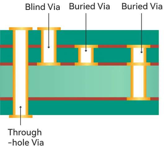
Sequential lamination vias
Explore how sequential lamination vias enhance signal integrity for high-frequency applications and reduce PCB layers for cost savings.



Explore how sequential lamination vias enhance signal integrity for high-frequency applications and reduce PCB layers for cost savings.
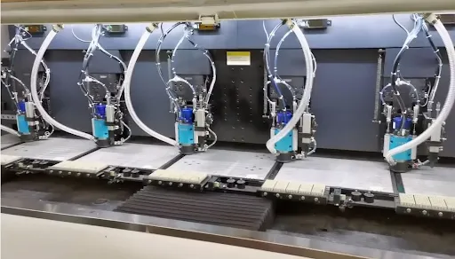
Master PCB drilling with tips on drill bits, laminate materials, and drill file prep. Ensure precision in manufacturing with this guide from ALLPCB.
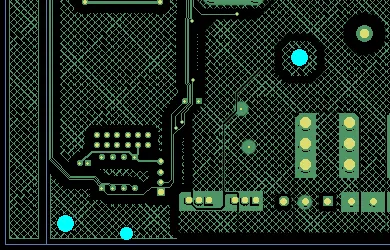
Explore copper balancing vs. copper pouring in PCB design. Learn which method suits your project for optimal performance and manufacturing.
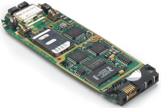
Learn mobile phone PCB repair with tips on short circuit fixes, trace repair, component replacement, multimeter testing, and rework stations.
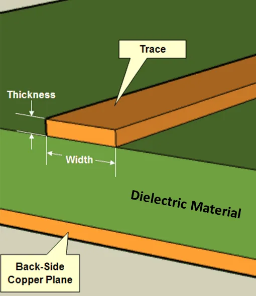
Learn to balance copper thickness and trace width for optimal PCB performance, focusing on current capacity, impedance, and signal integrity.

Explore silk screen color printing methods for PCB manufacturing. Compare techniques to find the best for electronics production needs.

Explore how thermal simulation software aids PCB designers with tools like ANSYS Icepak for heat management and reliable designs.

Explore OSP vs HASL and ENIG in this PCB finish comparison. Find the best surface finish choice for your DIY electronics project with our guide.
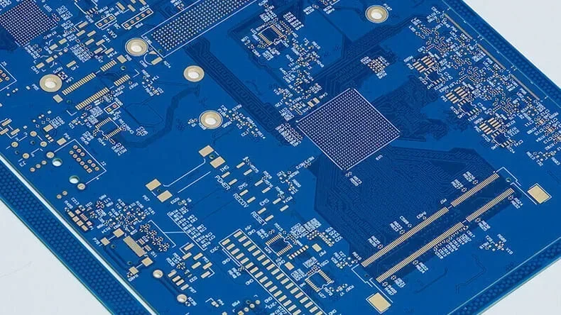
Explore HDI manufacturability and cost with insights on materials, layers, vias, and trace spacing for cost-effective PCB designs.
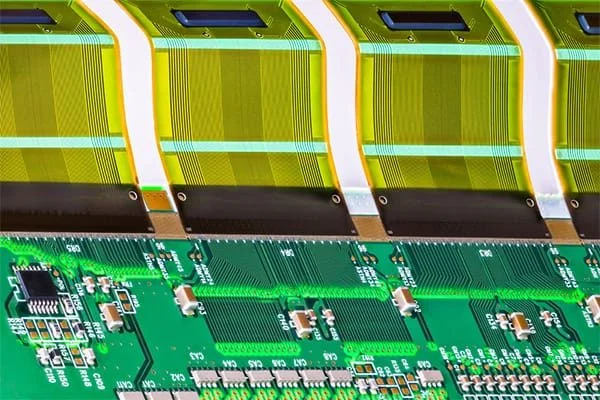
Explore Flex PCBs for reliability and blind/buried vias for cost savings in PCB design. Learn which is more common in manufacturing today.