 ALLPCB
BGA Breakout Design Rules: Ensuring Manufacturability and Reliability
Learn BGA breakout design rules for manufacturability and reliability, focusing on clearances and spacing for optimal PCB performance.



Learn BGA breakout design rules for manufacturability and reliability, focusing on clearances and spacing for optimal PCB performance.
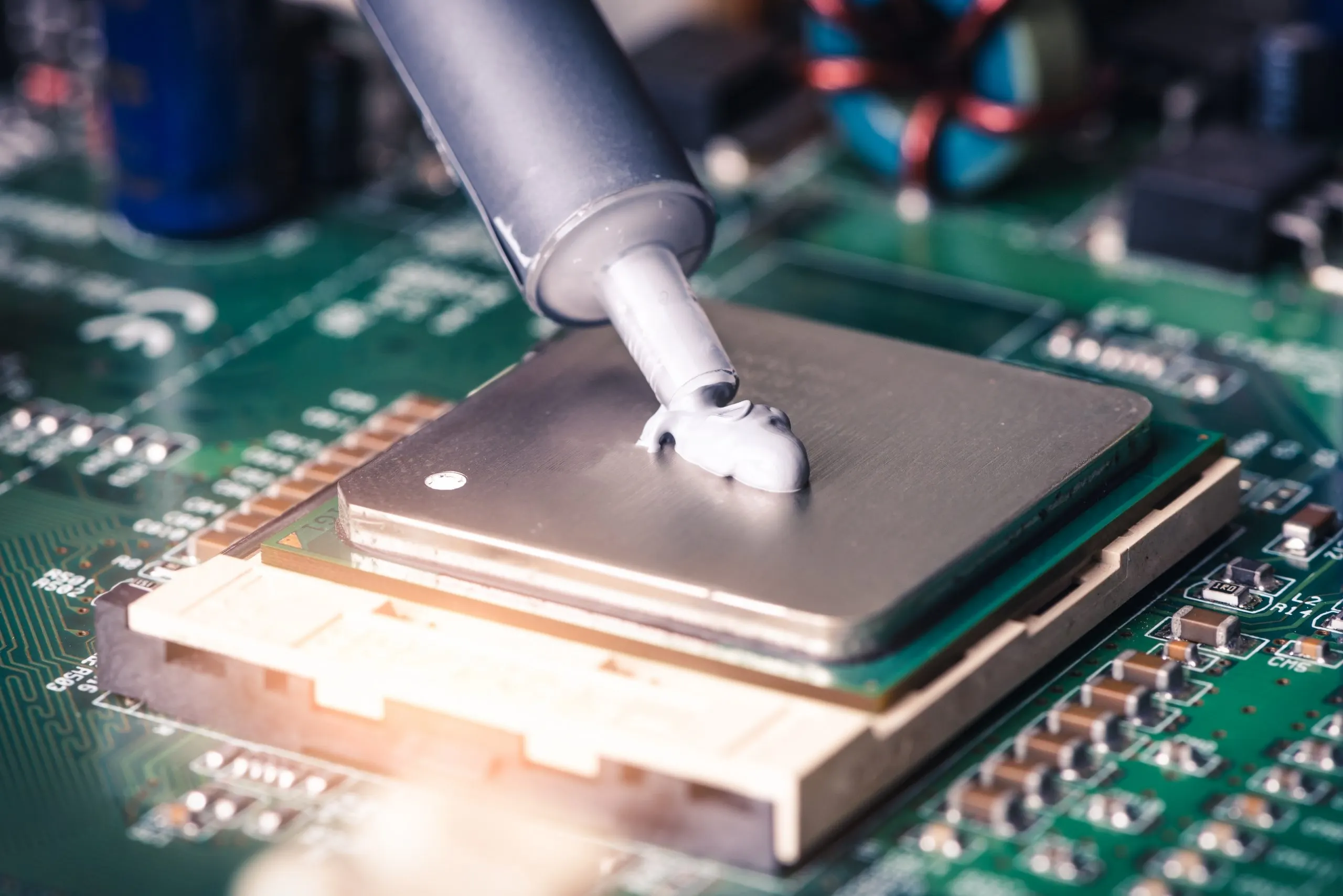
Optimize SMT thermal pad design for high-power components. This guide covers alignment, solder paste, reflow, and rework challenges to minimize assembly defects and enhance heat dissipation.
Explore a detailed comparison of rigid PCB materials like FR-4 and CEM. Learn their properties and choose the best for your design needs.
Learn strategic component placement to minimize crosstalk on a PCB. Optimize high-speed signals with expert layout tips for signal integrity.

Learn PCB impedance control with this easy guide for hobbyists. Get beginner design tips and DIY signal integrity advice for better PCBs!

Learn about Power Distribution Network (PDN) via placement for low impedance power delivery and EMI reduction in PCB design with expert tips.
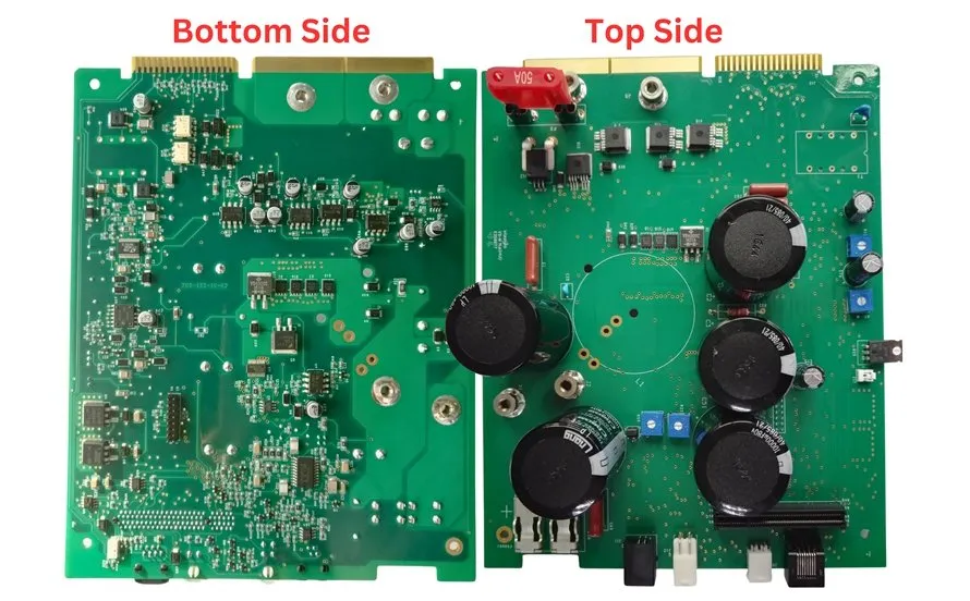
Explore the benefits and challenges of double-sided SMT assembly, including component placement, reflow soldering, and adhesive mounting tips.

Discover how advanced elevator PCB features like IoT control and predictive maintenance optimize performance, safety, and efficiency.

Discover essential tips for designing circuit board layouts as an electric hobbyist. Learn about PCB material selection and board fab notes.
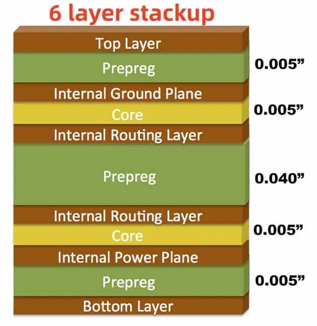
Explore advanced PCB routing techniques for multi-layer designs, including stackup, vias, impedance control, and high-density interconnects.
Master high-speed PCB layout with techniques for signal integrity, EMC compliance, controlled impedance, crosstalk reduction, and grounding.
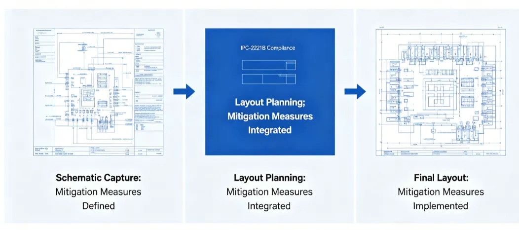
PCB ground bounce occurs due to inductance and fast switching currents on ground planes. The article explains the causes, effects on signal integrity, and mitigation strategies like solid planes and decoupling for improved PCB performance.
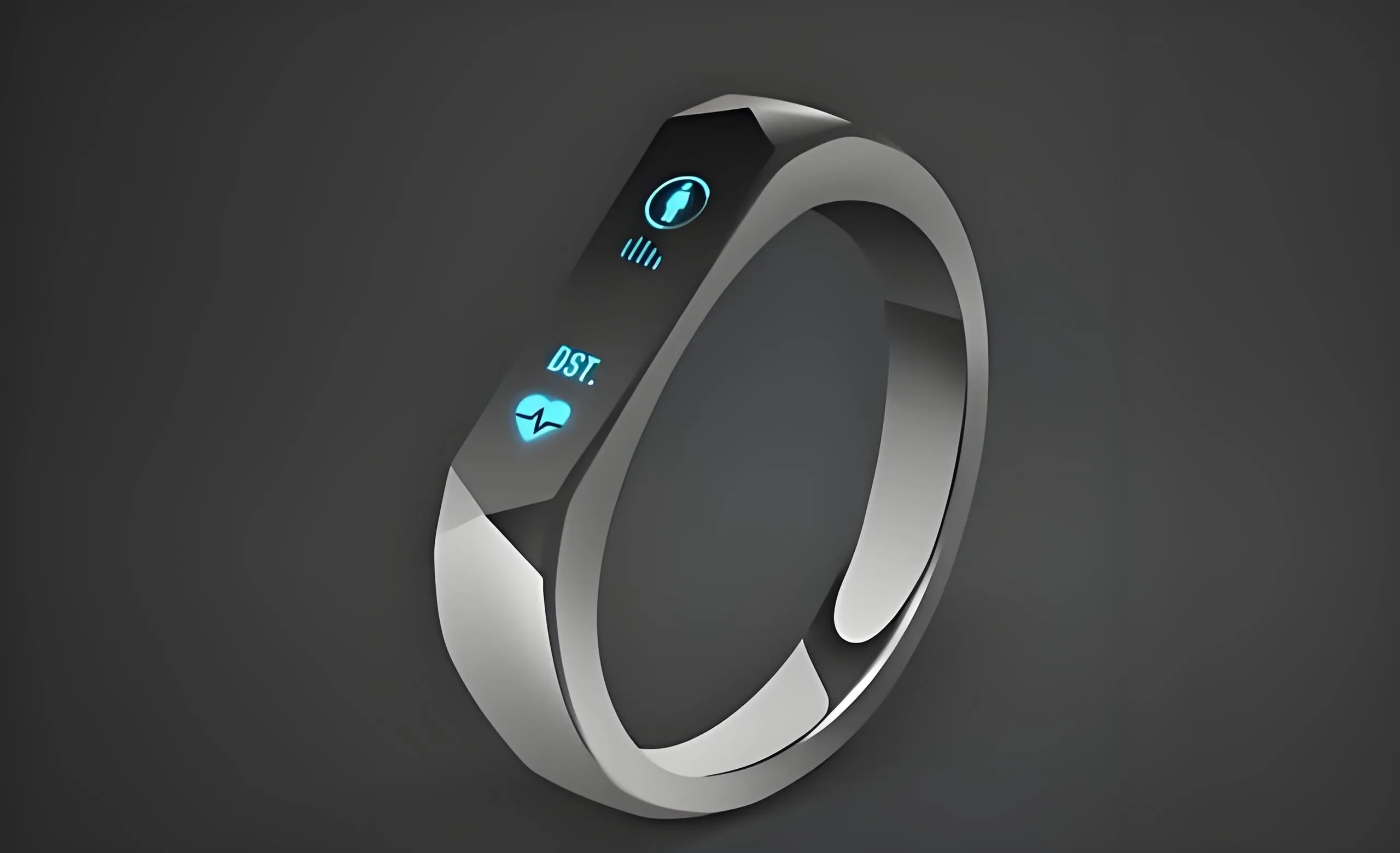
Explore the challenges of miniaturization and power efficiency in integrated circuits for wearable tech, with solutions for IC design and PCB innovation.

Discover fast, efficient RF PCB prototyping techniques with ALLPCB. Learn about quick-turn services, assembly, costs, and testing for your designs.

Explore if standard PCB dimensions exist in power electronics. Learn key factors, common sizes, and design tips for optimal layouts.

Learn best practices for through-hole PCB design reliability. Discover tips for robust through-hole design and build a reliable PCB with ALLPCB.
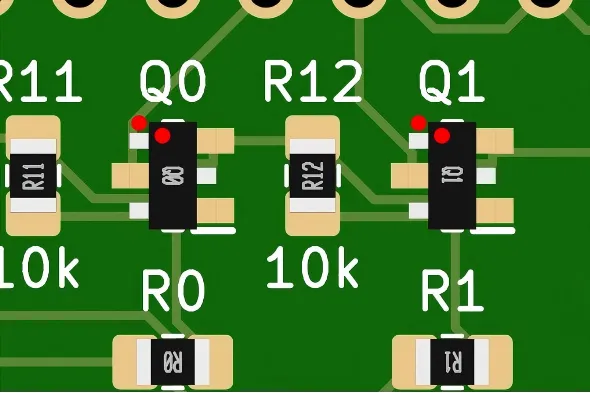
Learn PCB component placement strategies to maximize performance and reduce noise. Explore tips for high-speed designs and orientation.
Learn essential PCB grounding techniques for high-power boards to ensure reliable, safe electronic designs with minimal noise and EMI.

Learn through-hole grounding and power distribution for PCBs. Optimize designs with ground planes and practical tips for reliability.
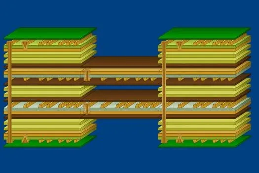
Master rigid-flex PCB design with our guide on flex-to-rigid transitions. Learn best practices and tips for reliable interfaces in this tutorial.